Cn

Mobile Phone: 18013061176

Applications
Applications

Key Words: PCB DepanelingLaser Marking Medical DeviceCover layer film cuttingHandheld Laser Welder

Home > 3C Electronic Fabrication

Printed Circuit Board (PCB) Fabrication

| Application


From single sided to multi-layer, double sided PCB designs in both rigid and flexible circuits (FPC), Chanxan Laser Technology has been an integral partner in advancing our customers’ manufacturing capabilities and product technology.


Our customers make up some of the largest international PCB manufacturers, original equipment manufacturers (OEM), and electronics manufacturing services (EMS) companies that serve the medical, electronics, telecommunications, industrial, communications, transportation, automotive, commercial and military sectors. 


Having supported most every industry across thousands of electronic products and applications, our contract laser services are a cost effective solution to producing IPC compliant electronic circuit boards.


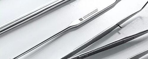
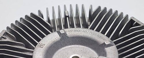
Circuit boards and electronic components are marked with permanent, solder-resistant and machine-readable laser markings, in order to guarantee accurate identification and traceability, which in turn guarantees a flawless quality assurance process across the entire life cycle chain and the process. 

Typical marking contents range from complex 2D-data matrix codes to alphanumeric characters and customized contents.


Housing


Electronic housing with laser marking (© Phoenix Contact GmbH & Co. KG)


  • simple alphanumeric codes

  • complex 2D codes, logos or customized data.


The quality of the markings is high, the imprinted characters are easy to trace and most of the materials that are used to build housings can be marked with the laser.

Electrical Material

Electrical Material

Electricity meter housing with individualized barcode


The black coating layer that is applied to the lower part of an electricity meter’s aluminum housing is removed, and the marking becomes visible as an individual barcode.


The barcode that is applied with the help of a laser is machine-readable and can be read by a scanner.

SMD component


SMD components are getting smaller and smaller, along with the markings that they carry, which must be applied with a high degree of precision. Since most components are microscopically small, the data contained in the marking seldom exceeds the micrometer range.


*The image to the right shows a relatively large microchip with a perfectly readable identification on its 4 mm x 4 mm marking surface. The marking time was 45 ms.

Electrical Material
Electrical Material


Printed circuit board


Typical marking contents range from complex 2D-data matrix codes to alphanumeric characters and customized contents.


Electrical Material


Electrical Material

| Second, the solution

image.png

FPC gold finger open skylight FPC is a printed circuit board made of a flexible substrate and has a pattern with high wiring density, light weight, and thin thickness. FPC is mainly used in mobile phones, notebook computers, PDAs, digital cameras, LCM and other products. It is especially suitable for applications with complicated circuits, high signal processing requirements or special electrical or mechanical performance requirements. The disadvantages of traditional processing methods For FPC cutting, the traditional method of processing is to use open molds, and then mechanical stamping through the mold. This processing method is a contact-type machining method, so it will inevitably have some deficiencies:


● As the circuit density and pitch of FPC products continue to increase, and the profile of FPC graphics becomes more and more complex, this makes it increasingly difficult to make FPC molds. For a typical FPC, it is difficult to make molds and the production cycle becomes longer, which results in a significant increase in processing costs. For highly complex FPCs, this very complicated mold making cannot be realized, so it is necessary to consider More sophisticated methods are used to cut these complex FPCs.

● Due to the insufficiency of machining, the FPC mold produced cannot reach a high precision surface, which restricts the further improvement of the FPC processing accuracy. At present, general mold processing can achieve an accuracy of ±50 μm, and it is very difficult or even impossible to achieve an accuracy of ±20 μm or less.

● As the traditional FPC cutting process is a contact-type machining method, it will inevitably cause processing stress on the FPC and may cause physical damage to the FPC. At the same time, when the covering film is subjected to a windowing operation by means of machining, it is inevitable that burrs and overflows will be generated in the vicinity of the window, and the burrs and the overflowing glue are very good after lamination, lamination, and bonding on the pad. Difficult to remove, directly affect the quality of the coating

| Free solution

| Related Products