Home > News > Company News
【Description】:
Laser annealing is used on all metals that show a color change when exposed to heat and oxygen.
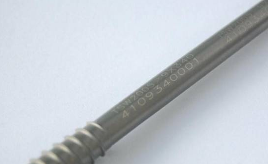
Laser annealing is used on all metals that show a color change when exposed to heat and oxygen. Laser marking selectively heats small areas of the workpiece surface until the annealed color appears. Annealing leaves the surface of the material free of scratches, but still produces high contrast, clearly identifiable marks.

Independent of material and marking method, laser marking offers almost limitless possibilities in marking content and shapes. The flexible software-controlled process allows for personalized marking content and dynamic marking of moving parts.
The use of laser annealing to redistribute the impurity ions injected into the silicon material and activate the impurities to improve the corresponding electrical properties has been applied to silicon solar cells in the early days.
After laser irradiation, nano-scale ripples or micro-scale cone structures can be generated on the silicon surface. Laser pulses scan on the silicon surface to achieve large-area laser-induced roughening, which is very suitable for industrial large-scale applications.
With the continuous growth of market demand for LTPS products and the continuous maturity of LTPS manufacturing technology, laser annealing technology plays an increasingly important role in the field of flat panel displays.
Laser annealing is used as an important basic method in the field of flat panel display, which is used to convert amorphous silicon films deposited on glass substrates into crystalline silicon films to prepare low-temperature crystalline silicon panels.
The application of laser annealing technology in integrated circuits is mainly in the following three aspects:
(1) anneal the electrodes (source, drain, gate) of the semiconductor device, and metallize to form an ohmic contact;
(2) Anneal the connections inside the integrated circuit;
(3) Annealing 3D structures, such as memory, NEMS, etc.
| Free solution