





The demand for precision glass cutting has grown exponentially across industries—consumer electronics, display manufacturing, semiconductor packaging, and optical component fabrication. Traditional mechanical methods—diamond scribing, wheel cutting, and abrasive sawing—have long been industry standards, but they come with inherent limitations: edge chipping, micro-cracks, subsurface damage, and the need for extensive post-processing such as grinding and polishing.
Picosecond laser technology has fundamentally changed this landscape. Its ultra-short pulse duration (<10 ps) enables cold ablation—material removal with negligible heat diffusion. The thermal effect on the workpiece is minimal, delivering a combination of precision, speed, and edge quality that traditional methods cannot match.
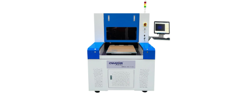
Core Process Advantages of Picosecond Laser Glass Cutting
1. Ultra-High Accuracy and Minimal Kerf Width
| Parameter | Typical Performance | Engineering Significance |
|---|---|---|
| Positioning accuracy | ±3 µm | Ensures cut placement matches design specifications. |
| Repeat positioning accuracy | ±2 µm | Guarantees consistency across high-volume production batches. |
| Kerf width | 3–5 µm | Minimises material waste—critical for expensive glass substrates. |
| Edge chipping | ≤10 µm | Often acceptable for direct assembly without secondary processing. |
The focused laser spot achieves power densities high enough to vaporise material directly. As the beam moves relative to the workpiece, it forms a continuous, narrow slit. Compared to mechanical cutting (kerf typically >100 µm) or waterjet cutting, the narrow kerf of picosecond laser significantly reduces material loss—particularly valuable for OLED glass, optical glass, and semiconductor wafers.
2. Superior Edge Quality – Smooth, Burr-Free, Crack-Free
| Quality Attribute | Picosecond Laser Cutting | Conventional Mechanical Cutting |
|---|---|---|
| Edge roughness | Smooth, burr-free | Rough, with burrs |
| Micro-cracks | None | Common |
| Subsurface damage | None | 30–100 µm |
| Heat-affected zone (HAZ) | Negligible to none | Significant (thermal methods) |
Because picosecond laser processing is non-contact and based on cold ablation, the cut edge is free from mechanical stress and thermal damage. This is particularly critical for ultra-thin glass (UTG) and display panel glass, where any thermal or mechanical stress can cause fracture. The cut surface typically requires no secondary processing and is ready for assembly or coating.
3. High Cutting Speed
| Speed Parameter | Typical Value |
|---|---|
| Linear cutting speed | Up to 500 mm/s |
| Corner cutting speed | Up to 300 mm/s |
Picosecond laser cutting is significantly faster than wire EDM and other conventional methods. High speed translates directly into high throughput, making it suitable for high-volume production environments.
4. Process Flexibility – Any Shape, No Tooling
| Capability | Description |
|---|---|
| Shape types | Straight lines, curves, inner and outer contours, complex profiles, holes |
| Design changes | Software-defined, instant modification |
| Tooling investment | Zero – no physical molds or tools required |
Picosecond laser cutting is driven by CAD/CAM software, with no tool geometry constraints. This delivers two key advantages:
Rapid iteration: Design changes require only software updates—no tooling replacement costs or delays.
Small batch economy: No mold amortisation cost makes prototyping and medium-volume production highly cost-effective.
5. Non-Contact and Low Thermal Impact – Zero Workpiece Damage
| Damage Type | Picosecond Laser Cutting |
|---|---|
| Scratches | None (no physical contact) |
| Mechanical stress fractures | None (no cutting force) |
| Thermal deformation | None (cold ablation) |
| Surface contamination | Minimal (dry process with assist gas) |
The non-contact nature of laser processing is particularly valuable for coated or polished glass surfaces, where any scratch would compromise optical performance or coating adhesion.
6. Wide Thickness Range
| Capability | Performance |
|---|---|
| Typical thickness range | 0.03 mm (30 µm) to 3 mm |
| Maximum cutting thickness | Up to 10 mm (depending on glass type and parameter optimisation) |
This broad thickness capability makes picosecond laser a truly versatile platform—from ultra-thin glass (<100 µm) for flexible displays to thick observation windows (several millimetres) for industrial applications.
Key System Characteristics
1. High Electro-Optical Conversion Efficiency
| Parameter | Specification | Benefit |
|---|---|---|
| Electro-optical efficiency | >30% | Significantly higher than conventional lamp-pumped lasers. |
| Power consumption | Lower | Reduces operating costs and cooling requirements. |
| Production efficiency | Highest | Maximum output per unit of energy consumed. |
2. No Additional Gas Required
No laser gas required (unlike CO₂ lasers).
No gas cylinder replacement or maintenance costs.
Simplified facility requirements.
3. Excellent Beam Quality and Wavelength Advantage
| Parameter | Specification | Significance |
|---|---|---|
| Output wavelength | 1.064 µm (IR) | 1/10 of CO₂ laser wavelength. |
| Beam quality | M² <1.3 (high) | Enables tight focusing and high power density. |
| Material absorption | Effective in both glass and metals | Versatile – capable of cutting, drilling, and welding. |
The combination of shorter wavelength and excellent beam quality enables efficient processing of transparent glass (through nonlinear absorption) and metals—extending equipment application range.
4. Protective Optics Design
| Component | Feature | Benefit |
|---|---|---|
| Cutting head | Integrated protective lenses | Shield focusing optics from debris and spatter. |
| Focusing lens life | Extended lifespan | Significantly extends lens lifespan and reduces maintenance downtime. |
Protective lenses are relatively inexpensive consumables, saving the higher cost of focusing lens replacement and reducing downtime.
Typical Application Scenarios
| Industry | Typical Workpieces | Key Laser Advantage |
|---|---|---|
| Consumer Electronics | Smartphone cover glass, watch faces, camera windows, sensor covers | High precision, zero chipping, high speed, arbitrary shapes. |
| Display Manufacturing | OLED/LCD panel glass, touch sensor substrates, UTG | Particle-free cutting, smooth edges, suitable for hermetic sealing. |
| Automotive | Central infotainment displays, instrument clusters, HUD combiners | Large-format cutting, high edge strength, thermal cycle resistance. |
| Optics & Photonics | Optical windows, lenses, filters, prism blanks | Zero taper, smooth surfaces, preserves optical performance. |
| Semiconductor & Packaging | Glass wafers, interposers, TGV substrates | Low thermal impact, high precision, meets advanced packaging requirements. |
| Medical & Laboratory | Microfluidic chips, diagnostic substrates, custom glassware | Complex geometries, clean edges, no tooling costs. |
| Precision Instruments | Measurement device windows, industrial display interfaces | High accuracy, consistent quality, no secondary processing. |
Chanxan Integrated Solution – IR Picosecond Cutting with CO₂ Laser Splitting
For manufacturers seeking an industrial, high-throughput glass cutting solution, Chanxan offers a uniquely integrated system: the Single/Dual-Station Picosecond Glass Laser Cutting and Splitting Machine.
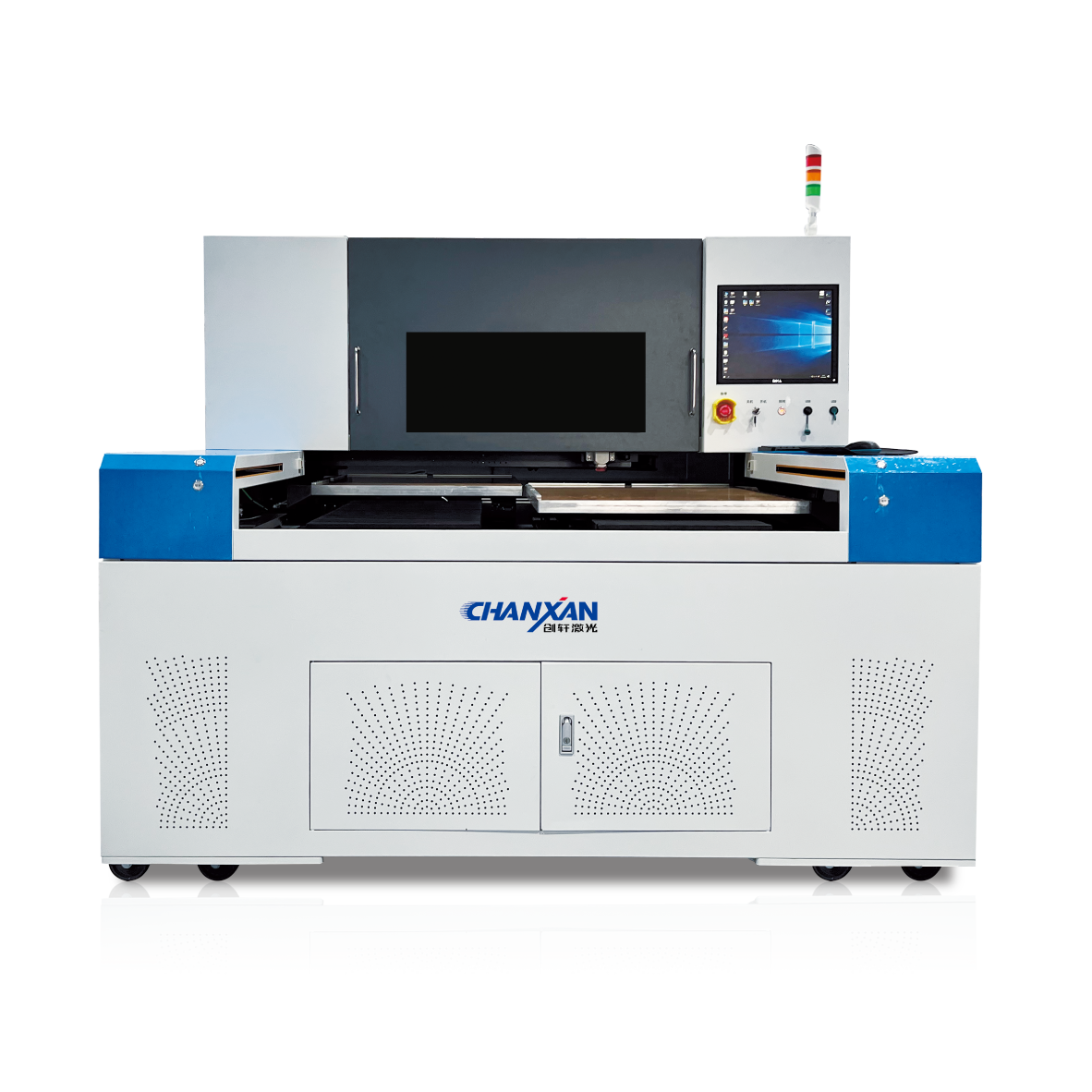
The system leverages the physical strengths of different laser wavelengths in a complementary manner: an infrared picosecond (IR ps) laser performs high-speed internal modification and contour definition, while a CO₂ laser executes controlled thermal splitting along the modified path.
Core Principle and Performance Advantages
| Step | Technology | Function |
|---|---|---|
| 1. High-speed modification | 70W IR picosecond laser | Creates uniform, controllable filamentation layer inside glass, defining precise cutting path. |
| 2. Precision splitting | 150W CO₂ laser | Scans rapidly along modified path, generating localised thermal stress for clean separation. |
Combined Benefits:
| Advantage | Description |
|---|---|
| Minimal chipping | ≤20 µm – superior to pure ablation processes. |
| Zero taper | Separation follows internal vertical modification layer – sidewalls are perfectly perpendicular. |
| Low thermal impact | IR ps "cold" modification + rapid CO₂ scan minimises HAZ. |
| High speed | Modification is fast; splitting is rapid – ideal for high-volume production. |
| Broad thickness range | 30 µm to 3 mm in a single pass. |
| Wide material compatibility | Optical glass, BK7, borosilicate, aluminosilicate (including strengthened), OLED/LED panel glass, fused silica, UTG, sapphire, and more. |
Key Specifications
| Parameter | Specification |
|---|---|
| Cutting laser | 70W IR Picosecond |
| Splitting laser | 150W CO₂ |
| Positioning accuracy | ±3 µm |
| Overall accuracy | ±15 µm |
| Chipping | ≤20 µm |
| Taper | Zero |
| Max thickness | 3 mm |
| Working area | Single: ≤500×500 mm; Dual: ≤600×900 mm |
| Motion base | High-rigidity granite/marble with multi-axis system (6-axis on dual) |
| Software | Chanxan self-developed – DXF/DWG direct import, process database, parameter-to-job binding |
Positioning vs. Pure UV Ablation
| Aspect | Chanxan IR ps + CO₂ Splitting | Pure UV Picosecond Ablation |
|---|---|---|
| Processing speed | Significantly faster – especially for thick glass and complex contours | Slower – material removal is layer-by-layer, time increases with thickness |
| Edge quality | Chipping ≤20 µm, zero taper | Excellent (Ra <0.5 µm), but may exhibit slight taper |
| Thickness capability | Optimised for 0.03–3 mm in a single pass | Best for thin to medium thickness (<1 mm); thick glass requires many passes |
| Throughput | High | Moderate to low for thick substrates |
| Capital investment | Higher (dual-laser integration) | Lower (single laser source) |
| Cost per part | Lower at high volumes | Higher for thick glass due to cycle time |
| Ideal application | High-volume production of display panels, automotive glass, and precision electronics components. | Prototyping, intricate micro-features, and thin glass substrates (<1 mm). |
Looking for Advanced Glass Laser Cutting Solutions?
Contact Chanxan Laser today to discuss your application requirements, request free sample testing, or get a customized quote for our high-precision picosecond laser systems.
Get a Free Quote & Consultation



