Key Words: Silicon Wafer Dicing PCB Depaneling Glass Cutting
Home > News > Company News
【Description】:
Discover how Chanxan non-destructive laser scribing achieves low-temperature, burr-free silicon wafer cutting to maximize chip strength and manufacturing yield.
Few consumer technologies illustrate the value of precision laser cutting as clearly as the fingerprint recognition module inside a modern smartphone. The silicon wafers used in these fingerprint sensors are produced using UV laser cutting, and the sapphire cover layer found in devices like the iPhone is separated using a related laser cutting process. Together, these two material-specific processes — plus the FPC (flexible printed circuit) soft-and-hard board material used in the fingerprint module assembly — depend on laser cutting technology capable of one-time forming at high speed to keep pace with smartphone production volumes.
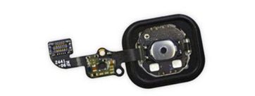
The technical demands here are unforgiving. A fingerprint recognition module chip, along with the camera modules manufactured alongside it, requires very high cutting precision, a smooth cross-section, and minimal chipping at the cut edge. Any deviation shows up directly as reduced sensor accuracy or reliability issues in the field. For cuts that need to satisfy all of these criteria simultaneously, laser cutting has proven to be the best available choice — mechanical alternatives simply cannot match the combination of precision and edge quality required.
A particularly notable development in this space is non-destructive laser scribing, which differs meaningfully from conventional laser scribing processes. In conventional laser scribing, high-temperature ablation is used to remove silicon material directly along the dicing track, which inevitably generates a large amount of silicon dust as a byproduct. Non-destructive laser scribing avoids this high-temperature ablation step entirely, and the practical benefits are significant:
The scribed section of the silicon wafer comes out clean, with no damage points, precisely because there's no high-temperature ablation degrading the material at the cut.
Dust generation drops dramatically compared to conventional scribing, since there's no bulk removal of silicon along the dicing track.
The process operates in a genuinely low-temperature range — roughly 180°C to 250°C — rather than the extreme localized heating that ablation-based cutting requires.
Cell strength is preserved. Compared to positive (unscribed) cells, non-destructive laser-scribed cells show almost no strength reduction, whereas conventionally laser-scribed cells typically see strength drop by more than 10%.
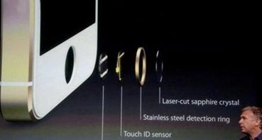
That strength-preservation point connects directly back to why laser cutting has become so central across semiconductor manufacturing more broadly. Just as quartz and glass benefit from reduced mechanical stress during cutting, and just as UV laser dicing of sapphire substrates avoids the chipping and reduced yield of mechanical cutter wheels, non-destructive silicon scribing avoids the strength degradation that comes with more aggressive, high-temperature laser processes. The common thread across every one of these applications is the same: minimizing damage to the material during separation directly improves the reliability, strength, and yield of the finished component.
For smartphone manufacturers and their component suppliers, this matters at scale. Fingerprint modules and camera modules are produced in enormous volumes, and even small improvements in yield or reliability compound into significant cost and quality outcomes across a production run. As mobile devices continue to push more sensors, cameras, and modules into increasingly compact form factors, the silicon and sapphire cutting processes behind these components will need to keep advancing in precision — and non-destructive, low-temperature laser scribing represents one of the clearest paths for doing so without sacrificing chip strength or reliability.
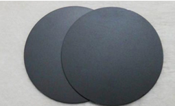
Seeking high-yield, low-temperature laser dicing solutions for silicon wafers or sapphire micro-processing?
Contact Chanxan Semiconductor Experts| Free solution
Previous: laser logo on ceramics