Home > News > Company News
【Description】:
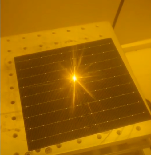
Laser precision cutting technology is used instead of wire cutting. Due to its non-contact processing and no stress, the cutting edge is straight and steam free, without damage, and the wafer structure will not be damaged, which improves the yield and reduces costs.
In the manufacturing process of crystalline silicon solar cells, laser cutting technology is mainly used for cutting wafer cutting and dicing cutting.
Laser precision cutting technology can be applied to scribing and cutting large-area cells, which can precisely control the cutting precision and thickness, further reduce cutting debris and improve battery utilization.

1) The laser can be focused into a small spot and can draw very thin lines.
2) The cutting depth is 2 to 3 times larger and can be controlled, which greatly improves the qualified rate of cutting.
3) Non-contact processing, the action time and action range of the silicon wafer are small, the heat affected zone is small, and cracks will not be caused by mechanical stress.

4) The dicing speed is fast, which greatly improves the productivity, is suitable for automatic control and online, and reduces the production cost.
5) It can scribe the semiconductor board plated with protective layer.
Wafer cutting is a key process in the production of monocrystalline silicon cells.
Laser precision cutting technology is used instead of wire cutting. Due to its non-contact processing and no stress, the cutting edge is straight and steam free, without damage, and the wafer structure will not be damaged, which improves the yield and reduces costs.
At the same time, the characteristics of small slit width, high precision, and adjustable laser power also enable the application of laser precision cutting technology to control the cutting thickness, thereby making it possible to achieve thinning of solar cells.
| Free solution