

Key Words: Silicon Wafer Dicing PCB Depaneling Glass Cutting
Home > News > Industry News
【Description】:
TGV vs. TSV – A Comprehensive Comparison of Through‑Glass Via and Through‑Silicon Via Technologies for Advanced Packaging
For over a decade, silicon interposers with Through‑Silicon Vias (TSVs) have been the industry standard, powering high‑end devices such as GPUs, FPGAs, and HBM memory stacks. However, as packaging demands diversify – particularly towards high‑frequency applications, large‑area chiplets, and cost‑sensitive modules – a compelling alternative has gained traction: glass interposers with Through‑Glass Vias (TGVs).
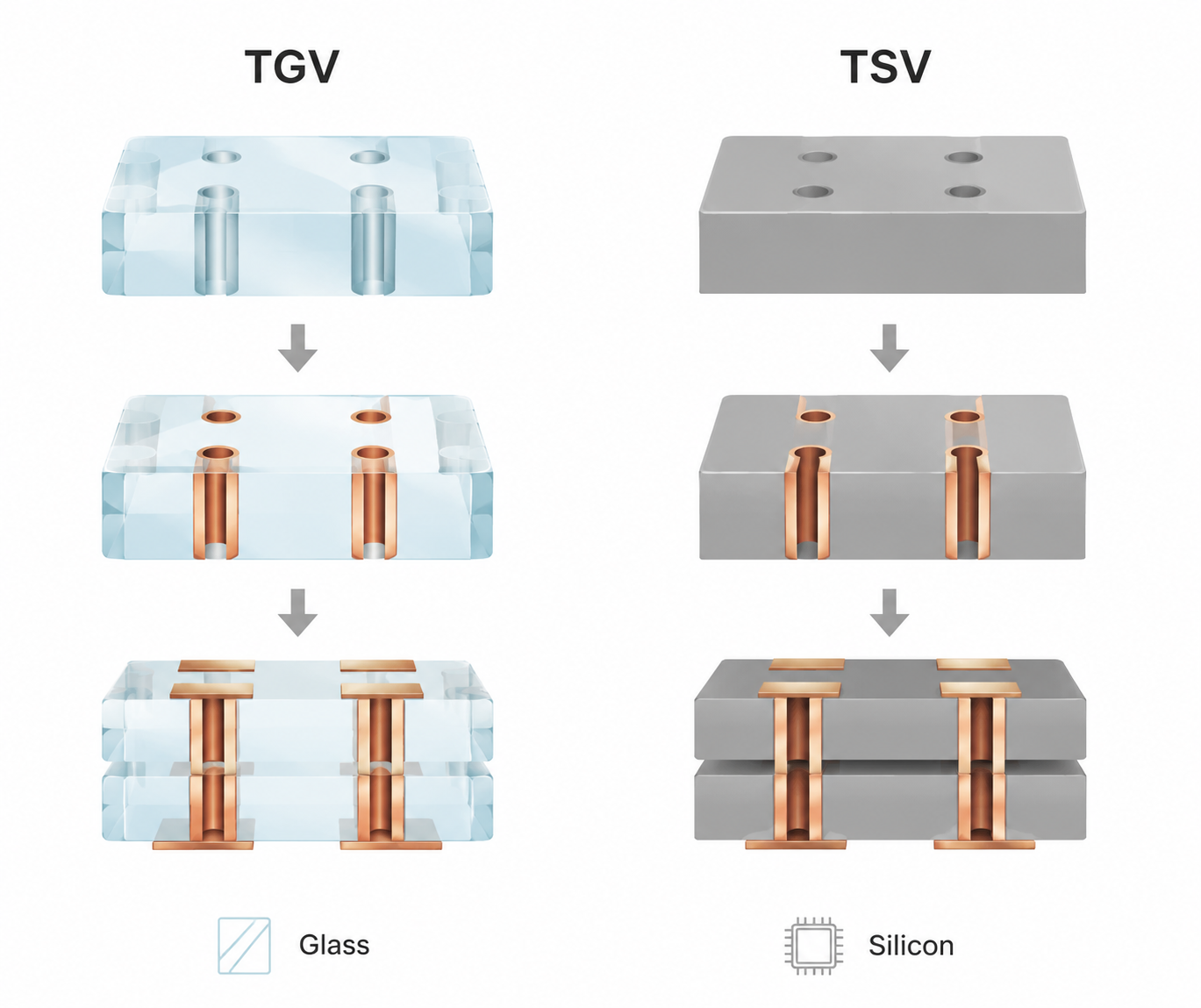
| Parameter | Through‑Glass Via (TGV) | Through‑Silicon Via (TSV) |
|---|---|---|
| Substrate material | Glass (borosilicate, fused silica, alkali‑free) | Silicon (single‑crystal) |
| Dielectric constant (Dk) | ~4.8 (low, stable) | ~11.9 (high) |
| Loss tangent (Df) | 0.002–0.005 (very low) | 0.01–0.02 (higher loss) |
| Electrical resistivity | >10¹⁴ Ω·cm (insulator) | ~10³ Ω·cm (semiconductor) |
| Insulation layer required | No – glass is inherently insulating | Yes – SiO₂ or Si₃N₄ to isolate from Si |
| CTE (ppm/°C) | 3–8 (tuneable to match Si or organics) | ~2.6 (fixed) |
| Thermal conductivity | ~1 W/m·K (low) | ~150 W/m·K (high) |
| Substrate thickness | 100–500 µm (can be thicker) | 50–300 µm |
| Via formation method | Laser drilling (ps/fs) + optional wet etch | DRIE (Bosch process) |
| Minimum via diameter | 30–50 µm (practical) | 5–30 µm |
| Aspect ratio | Up to 15:1 | Up to 20:1 |
| Sidewall quality | Smooth (Ra <0.5 µm) with ps laser | Scalloped – requires smoothing |
| Process complexity | Lower – fewer steps | Higher – multiple deposition and litho steps |
| Substrate size | Panel‑scale (up to 500×500 mm) | Wafer‑scale (300 mm max) |
| Cost per interposer | Lower (larger area, fewer steps) | Higher (wafer cost, complex processing) |
| RF / millimetre‑wave performance | Excellent – low loss, low crosstalk | Good – but limited by silicon loss |
| Optical transparency | Yes – enables optical alignment and integration | No |
| Maturity | Emerging – rapidly growing | Mature – high‑volume production |
| Primary applications | 5G/6G RF modules, automotive radar, photonics, chiplets, MEMS | High‑end computing, GPUs, HBM, FPGA, ASICs |
Silicon has a high dielectric constant (Dk ≈ 11.9) and a loss tangent (Df) of 0.01–0.02, which become problematic at frequencies above 10 GHz. Signal attenuation and cross‑talk increase significantly, limiting the use of silicon interposers in millimetre‑wave (mmWave) applications (e.g., 5G NR bands up to 52 GHz, automotive radar at 77 GHz).
Glass, by contrast, offers Dk ≈ 4.8 and Df as low as 0.002 – comparable to high‑performance organic laminates. This translates to:
Lower insertion loss – signals travel with minimal attenuation.
Reduced parasitic capacitance – because the substrate is not conductive, there is no depletion capacitance or leakage.
Better isolation – neighbouring vias or traces couple less, enabling denser routing.
Practical impact: For RF front‑end modules, antenna‑in‑package (AiP), and optical transceivers, TGV delivers significantly better signal integrity than TSV.
TSVs require a thick (typically 0.5–1 µm) SiO₂ or Si₃N₄ liner to electrically isolate the copper via from the conductive silicon substrate. This liner adds process complexity and capacitance. TGVs, because glass is an insulator, need no such liner – simplifying fabrication and reducing parasitic capacitance.
Silicon has excellent thermal conductivity (~150 W/m·K), making it an effective heat spreader. This is a major advantage for high‑power devices, as heat can be conducted through the silicon interposer to a heatsink.
Glass, with thermal conductivity of only ~1 W/m·K, is a poor conductor. Heat dissipation in glass interposers relies on the copper‑filled vias (which conduct heat better) and on external thermal management. For power‑hungry processors, silicon still has an edge.
Mitigation: For many RF and sensor applications, power densities are lower, so the thermal disadvantage of glass is less critical. For high‑power chiplets, hybrid designs (glass with embedded thermal vias) are being explored.
Silicon CTE is fixed at ~2.6 ppm/°C. Glass CTE can be engineered by adjusting the glass composition – typically from 3 to 8 ppm/°C. This tuneability is highly valuable:
Matching to silicon chips (CTE ~2.6–3.5 ppm/°C) minimises thermo‑mechanical stress at chip‑interposer interfaces.
Matching to organic substrates (CTE ~10–17 ppm/°C) reduces warpage in fan‑out packages and board‑level assembly.
Silicon's fixed CTE cannot be adjusted, which often leads to warpage issues when pairing with organic boards.
Via etching – Deep reactive ion etching (Bosch process) alternates etching and passivation, producing vertical via holes with characteristic scalloping.
Insulation liner deposition – thermal oxidation or CVD of SiO₂ to isolate the via.
Barrier/seed layer – PVD of Ti/Cu.
Copper fill – electroplating (bottom‑up fill).
CMP – removal of overburden copper.
Backside thinning – to expose the via.
Critical challenges: Scalloped sidewalls must be smoothed (often by oxidation/etchback), and the multiple deposition steps add cost and time.
Via drilling – laser drilling (picosecond or femtosecond) creates holes in the glass.
Cleaning – removal of debris and micro‑roughness (wet etch or plasma).
Barrier/seed layer – sputtering of Ti/Cu (no insulation layer needed).
Copper fill – electroplating.
Planarisation – CMP or grinding.
Thinning – optional backside grinding.
Key advantages: The laser drilling step is mask‑less, digital, and does not require vacuum or high‑temperature deposition for insulation. The sidewalls are smooth as‑drilled (with ps/fs lasers), eliminating the smoothing step.
TSV processing is performed on 200 mm or 300 mm silicon wafers. Each wafer yields a limited number of large interposers (e.g., for a 50×50 mm interposer, only a few per wafer).
TGV can be processed on large‑area glass panels (e.g., 500×500 mm), which are far more economical – significantly more interposers per panel, reducing the cost per interposer.
TSV requires 6–8 major process steps, including multiple high‑cost deposition and lithography steps. TGV requires fewer steps (no insulation liner deposition, no smoothing etch), reducing capital equipment and consumables.
Laser drilling of TGVs can achieve high throughput via multi‑beam or fast scanning, and the process is parallelisable across the panel. DRIE is a serial (wafer‑batch) process with longer cycle times for deep vias.
Overall, TGV interposers are significantly more cost‑effective for large‑area and mid‑volume production, while TSV remains competitive for very high‑density, small‑form‑factor designs where cost is secondary.
| Application Scenario | Recommended Technology | Rationale |
|---|---|---|
| High‑end CPUs/GPUs with HBM | TSV | Requires highest density, finest pitch, and excellent thermal management. |
| 5G mmWave RF modules | TGV | Low loss, low crosstalk, and transparency for optical alignment. |
| Automotive radar (77 GHz) | TGV | Superior RF performance and reliability in harsh environments. |
| Optical transceivers / silicon photonics | TGV | Glass transparency enables optical I/O integration; low loss. |
| Chiplet integration (large die) | TGV | Panel‑scale low cost; CTE tuneable to match multiple chip materials. |
| MEMS / inertial sensors | TGV | Glass provides hermetic sealing compatibility and low parasitic capacitance. |
| Cost‑sensitive consumer devices | TGV | Lower interposer cost, especially for large panels. |
| High‑density, fine‑pitch interconnects (<10 µm) | TSV | Laser‑drilled TGV currently limited to ~30 µm vias; TSV can go smaller. |
The practical viability of TGV depends entirely on the quality and efficiency of via drilling. Unlike silicon, glass cannot be etched anisotropically with standard plasma processes – it requires laser ablation.
Why picosecond UV lasers are the preferred choice:
Cold ablation – ultra‑short pulses remove material via photomechanical and photochemical mechanisms, with negligible heat diffusion.
No micro‑cracks – glass is brittle; thermal lasers (CO₂, ns IR) induce cracks that cause yield loss.
Smooth sidewalls – ps lasers produce Ra <0.5 µm, ready for barrier deposition without additional smoothing.
High aspect ratio – capable of producing vias up to 15:1 (e.g., 50 µm diameter in 750 µm thick glass).
High throughput – with galvo scanning and multi‑pass trepanning, thousands of vias per second are achievable.
Chanxan's role in enabling TGV manufacturing:
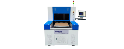
Chanxan CW‑6050PZ Picosecond Laser System (355/1064 nm) is purpose‑designed for TGV drilling. It delivers:
Precise drilling algorithms for vertical sidewalls.
Dynamic Z‑focus tracking to maintain focus as the via deepens.
Integrated debris evacuation for clean vias.
TGV and TSV are not strict competitors – they are complementary technologies suited to different requirements. TSV excels in ultra‑high‑density, high‑power computing applications where silicon's thermal conductivity and fine‑pitch capabilities are unmatched. TGV shines in high‑frequency, large‑area, cost‑sensitive, and optically integrated applications where glass's dielectric properties, panel scalability, and CTE tuneability provide clear advantages.
As advanced packaging continues to evolve, many designs may even combine both – using a glass interposer for RF and photonic interfaces alongside a silicon bridge for high‑speed digital links. The choice ultimately depends on:
Operating frequency and signal integrity requirements.
Power dissipation and thermal budget.
Form factor and chiplet size.
Cost targets and production volume.
For TGV, the critical success factor is the quality of the via – and that is where ultrafast laser drilling, particularly with UV picosecond lasers, becomes indispensable. Chanxan's picosecond laser system provides the precision, flexibility, and productivity needed to make TGV a viable, cost‑effective alternative to TSV for a growing range of applications.
| Free solution








