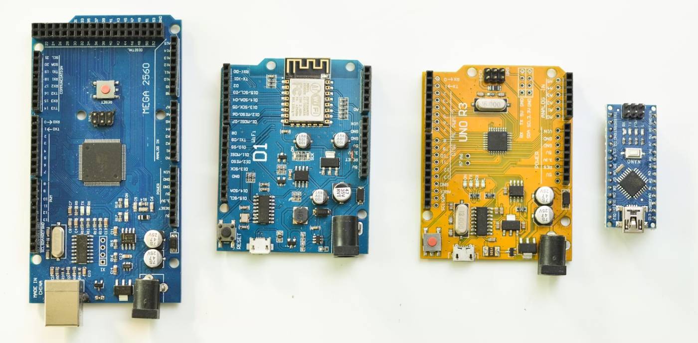
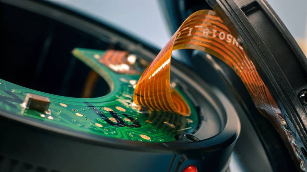
Precision Laser Equipment for Semiconductor Packaging, Electronics Manufacturing.
Laser Micromachining Solutions for Electronics Manufacturing
Advanced ultrafast laser solutions for cutting, drilling, marking, and surface processing in consumer electronics, semiconductors, and precision components.
Overview
Precision laser micromachining enables high-accuracy cutting, drilling, and patterning with minimal thermal damage across advanced materials such as glass, sapphire, silicon, and flexible substrates.
Widely applied in OLED/Micro-LED displays, Flex PCB manufacturing, and precision electronic components, Chanxan Laser empowers next-generation electronics manufacturing with advanced laser systems designed for precision, efficiency, and scalable industrial performance.

Applications & Material Compatibility
Engineered for diverse electronic manufacturing needs, Chanxan Laser solutions support precision processing across advanced materials and high-value applications.
Semiconductor Packaging
Optoelectronics
Precision Components
Consumer Electronics
Wearable Devices
AR / VR Devices
PCB / FPCB Processing
Display Manufacturing
Connector & Micro Assembly
Battery Electronics
Automotive Electronics
Medical Electronics
Comprehensive Solutions
1. Precision Structuring
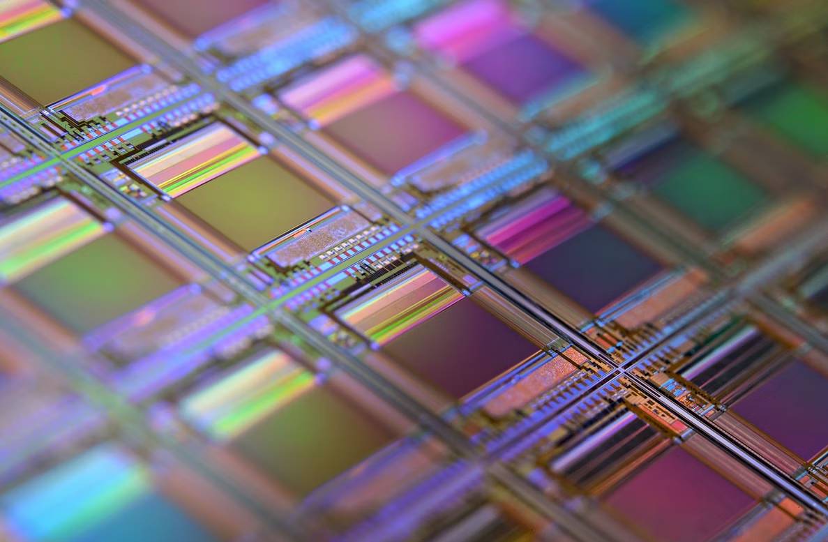
Precision Structuring creates high-precision microstructures on or within advanced electronic materials, achieving micron to nanometer scale features.
Key Processes
Laser Cutting
Laser Drilling
Laser Scribing
Precision Etching
Key Advantages
Micron-level processing accuracy
Minimal heat-affected zone (HAZ)
Non-contact processing
Excellent edge quality
Suitable for ultra-thin materials
Applications:
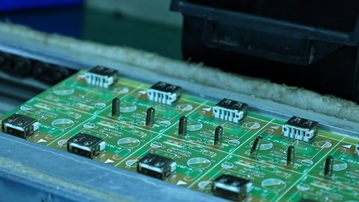
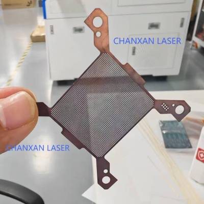
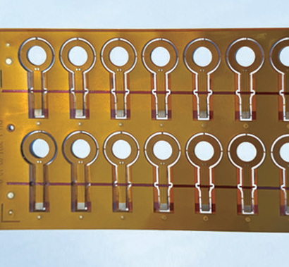
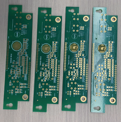
PCB & FPC Processing: High-precision cutting, depaneling, drilling, and thin-film processing for PCB, FPC, and flexible electronic components.
Micro-circuit Patterning: Precision laser patterning of ITO conductive films and flexible substrates for touchscreens, flexible displays, sensors, and advanced electronic circuitry.
OLED & Cover Glass Processing: High-precision structural processing of ultra-thin glass, sapphire, and flexible display materials.
Semiconductor Wafer Processing: Applicable for wafer dicing, substrate cutting, micro-drilling, and MEMS micromachining.
Optical Components: High-precision micromachining of microlens arrays, optical films, and diffractive optical elements for advanced optoelectronic and photonic devices.
2. Selective Layer Removal
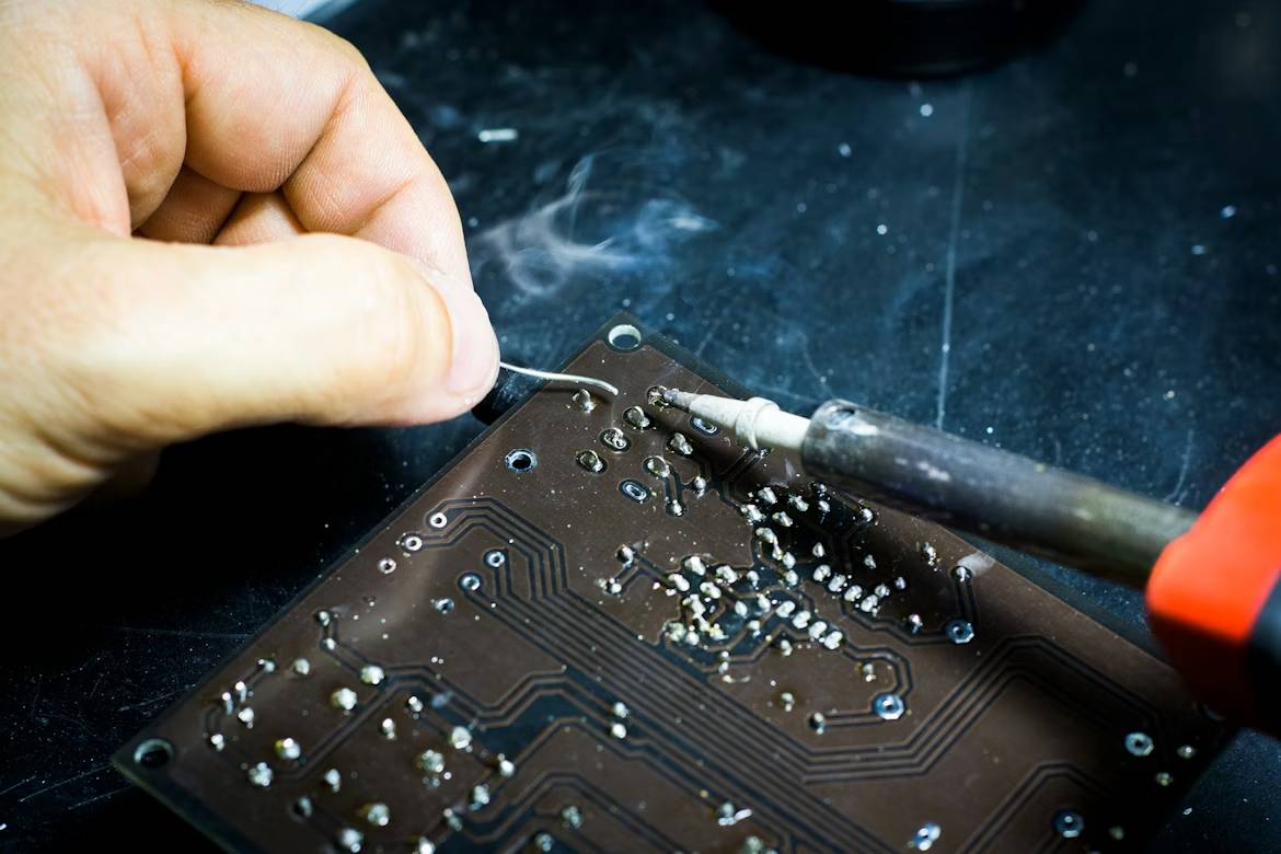
Selective Layer Removal technology uses high-energy density lasers to precisely remove specific functional layers, coatings, or films while maximally protecting the underlying substrate.
Key Processes
Laser Stripping
Coating Removal
Film Removal
Paint Removal
Key Advantages
High selectivity in processing
Precise control over removal depth
No damage to underlying materials
Reduced residue and contamination
Suitable for complex multi-layer structures
Applications:
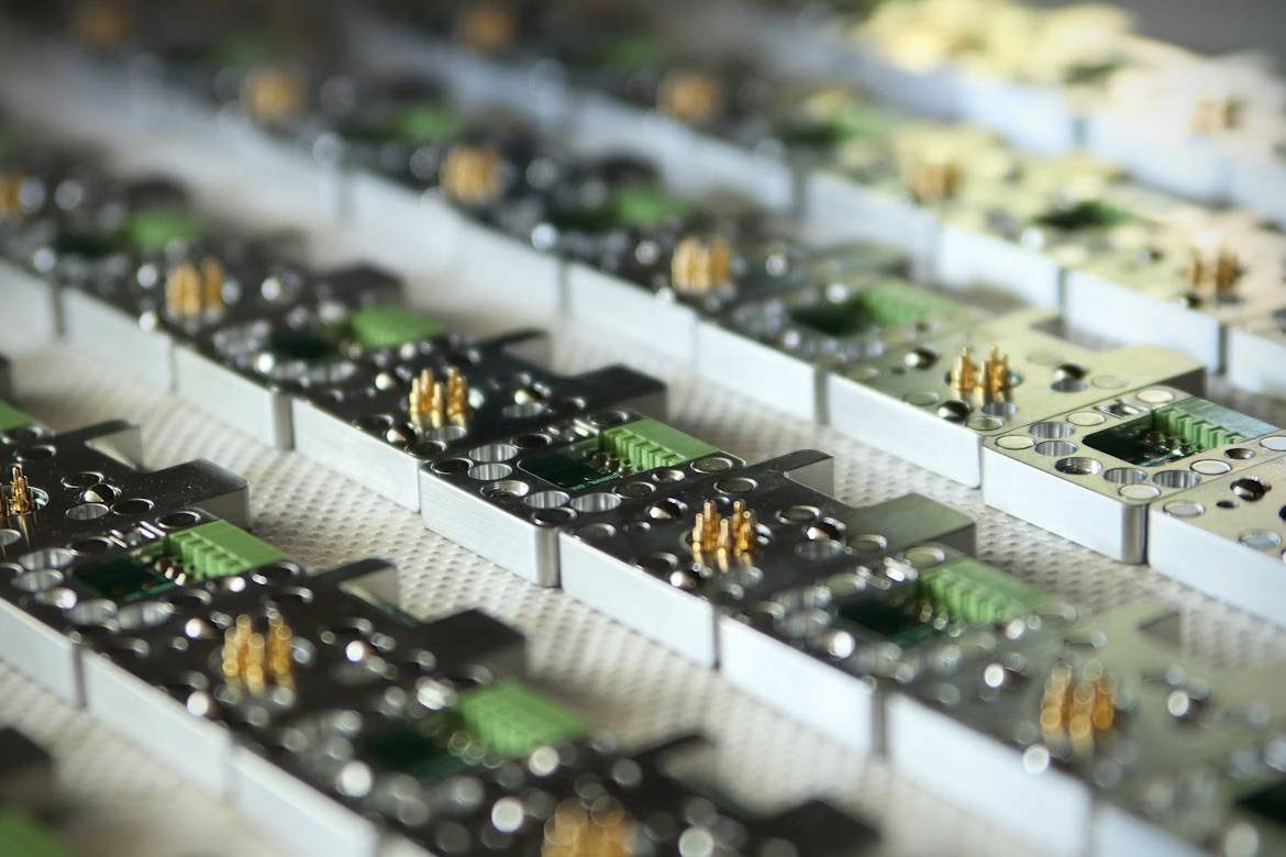
PCB/FPC Surface Processing: Selective removal of solder mask, insulating coatings, and surface layers for PCB/FPC.
Coating Removal: Removing localized coatings on chip lead frames for subsequent bonding or welding; Precisely removing coatings on battery electrode sheets and sensor electrodes to expose conductive materials.
Film Removal: Removing ITO, metal films for patterning displays and touchscreens; Removing localized protective layers for subsequent processing.
Paint Removal: Removing localized paint layers for translucent buttons and indicator light windows on electronic product casings; Removing solder mask for circuit board repair.
3. Surface Functional Processing
Surface Functional Processing enables enhanced performance, improved adhesion, and precision structuring.
Key Processes
Functional Etching
Surface Texturing
Surface Activation
Anodized Surface Processing
Electroplated Surface Processing
Key Advantages
Precise control of surface microstructures
Improved adhesion and surface energy
Enhanced heat dissipation and performance
Supports localized processing
Suitable for high-end requirements
Applications:
Precision Surface Structuring: Laser micromachining of semiconductor, glass, ceramics, and optical materials to create precision microstructures.
Surface Texturing: Micron-level surface texturing for thermal management components, heat sinks, and electronic parts.
Anodized & Coated Surface Processing: Precision laser processing of anodized aluminum, coated metals, and electronic housings for localized patterning, decorative features, functional marking, and selective coating removal.
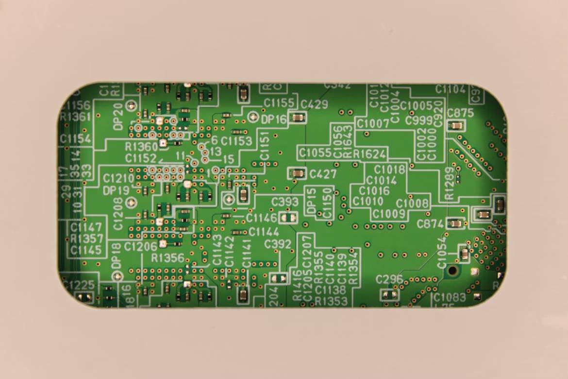
Precision Circuit & Layer Structuring: High-precision laser structuring of conductive layers and coated surfaces for fine circuitry, localized material removal, and electronic component processing.
4. Marking & Traceability
Laser marking technology creates permanent, high-contrast, and wear-resistant marks on various materials including metals, plastics, ceramics, glass, and composite materials.
Key Processes
QR / Data Matrix Marking
PCB Marking
Black Marking
Precision Engraving
Key Advantages
Permanent, high-contrast marking
Supports micro-sized encoding
High-speed online processing
Supports MES and automation
Excellent wear resistance
Applications:
QR/Data Matrix Marking: High-precision marking of micro QR codes, Data Matrix codes, serial numbers, and traceability identifiers on chips, PCBs, connectors, and electronic components.
PCB Marking: Marking serial numbers, logos, production dates, and traceability information on PCB, FPC, and electronic assemblies.
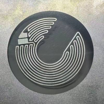
Black Marking: Creating high-contrast, tactile-free black marks on anodized aluminum casings of smartphones and laptops; Forming black marks on stainless steel surfaces for medical devices and precision tools.
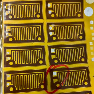
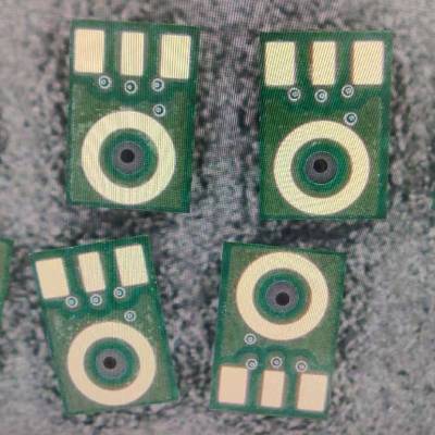
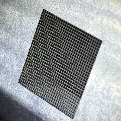
Sample Showcase
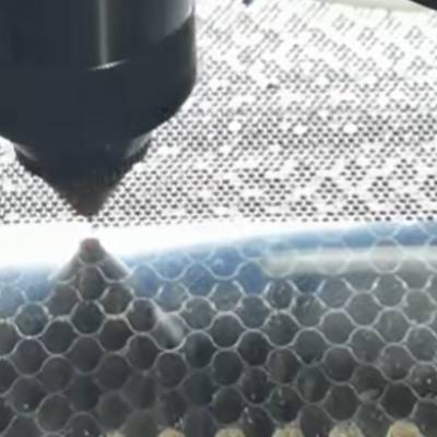
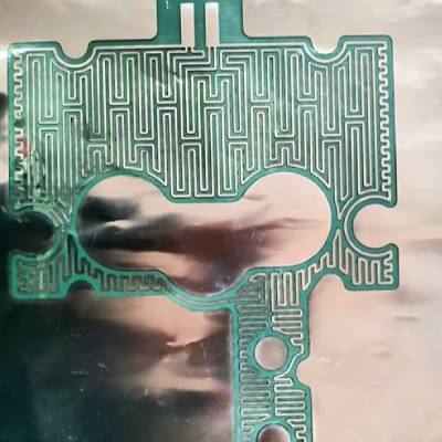
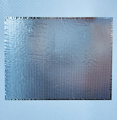
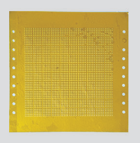
About Chanxan Laser

Precision Laser Processing Excellence
Chanxan Laser, with its profound expertise in precision laser processing, delivers premium laser equipment to the electronics manufacturing industry. Leveraging its mature process database and customized solution system, Chanxan Laser continues to drive electronic processing technology towards a more precise, intelligent, and efficient future.
We are committed to assisting clients in achieving an intelligent manufacturing upgrade characterized by "high precision, high efficiency, and high cost-effectiveness." We combine cutting-edge ultrafast laser technology with deep industry knowledge to solve complex manufacturing challenges.
With proven expertise across consumer electronics, wearable devices, PCB/FPCB, semiconductor packaging, display manufacturing, battery electronics, optoelectronics, precision components, connectors, automotive, medical, and AR/VR applications, ChanXan Laser stands as a trusted partner for precision laser processing solutions in the global electronics manufacturing industry.
Featured Products
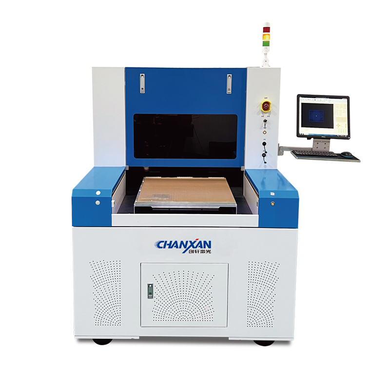
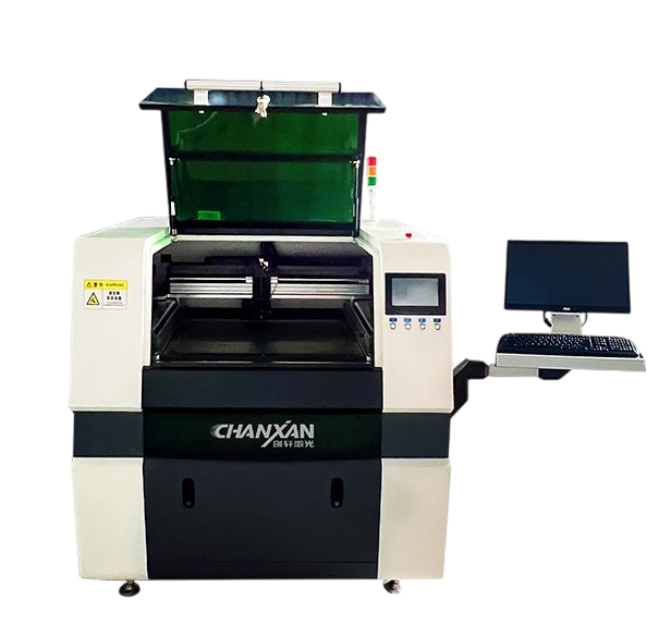
Femtosecond Laser Micromachining System
Ultrafast femtosecond laser machine for micromachining with minimal HAZ. Ideal for ceramics, metals, glass, and advanced materials.
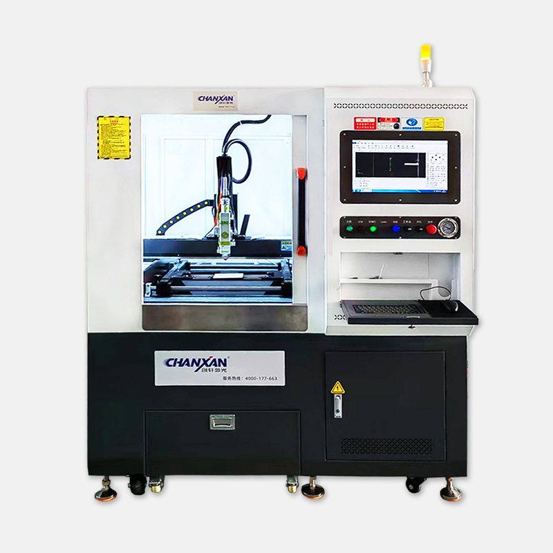
Learn More →Picosecond Laser Micromachining System
Picosecond laser system for high-speed precision cutting of FPC, PI film, and foils. Delivers stable micromachining performance.
Learn More →Nanosecond Laser Micromachining System
High-precision nanosecond laser system for PCB and FPC cutting.
Learn More →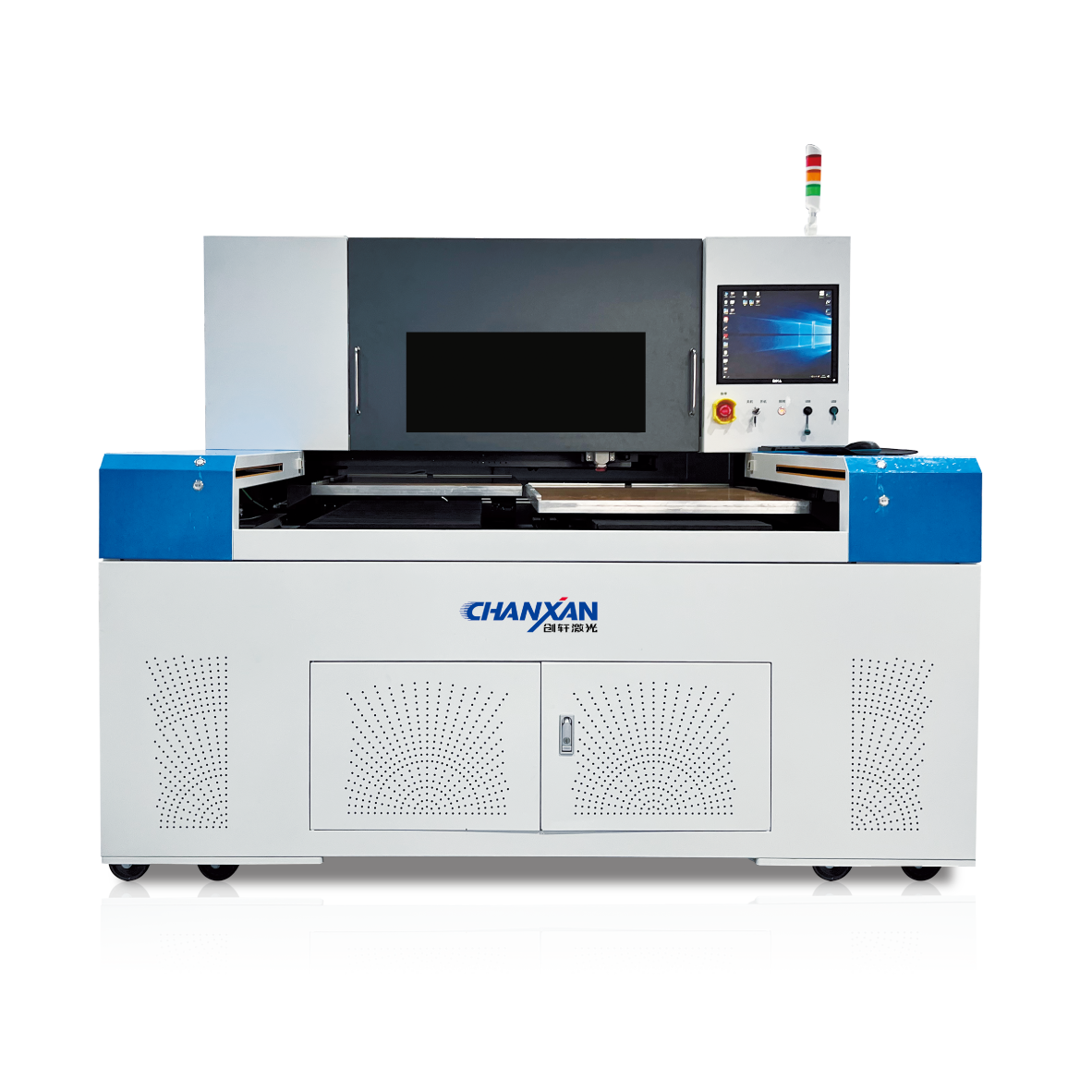
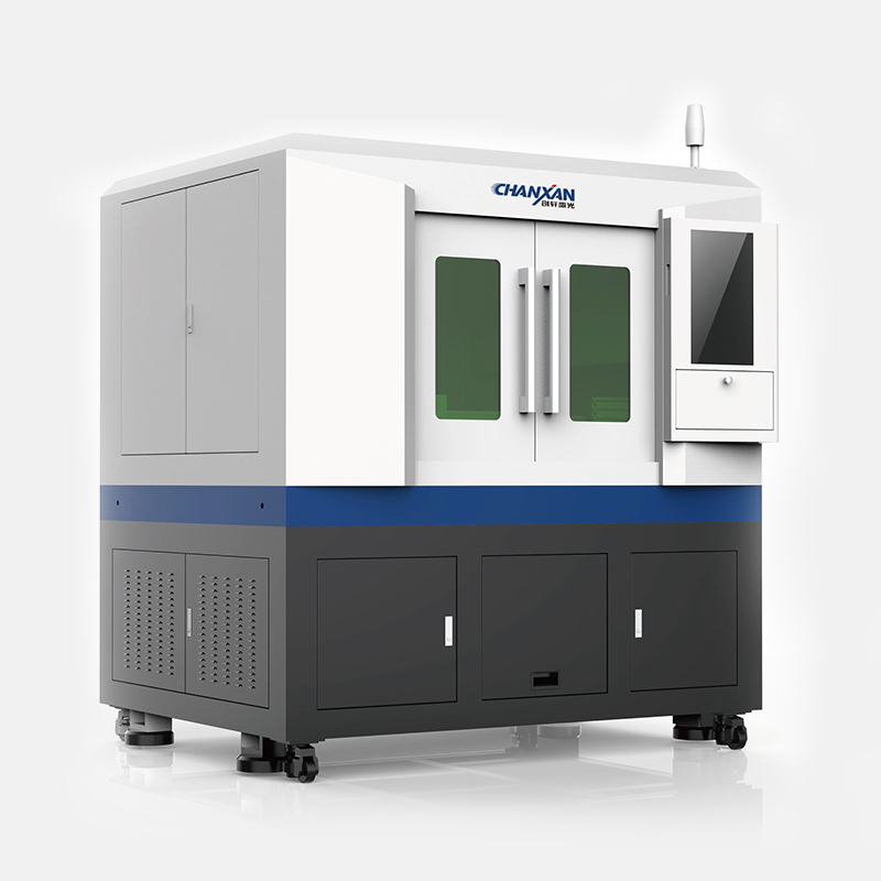
Picosecond Glass Laser Cutting and Splitting Machine
Picosecond laser system for glass and sapphire cutting and drilling. Ideal for panels and semiconductors.
Learn More →Trusted Partners
Master of Laser Precision Machining for the Chip Era
Partner with Chanxan Laser to achieve higher precision, faster production, and reliable ultrafast laser processing solutions for next-generation electronic manufacturing.
Contact Our Experts| Free solution