Key Words: Silicon Wafer Dicing PCB Depaneling Glass Cutting
Home > News > Industry News
【Description】:
A technical guide to laser fiducial marking on PCBs, FPCs, semiconductor packaging, glass, and ceramics, covering laser selection, critical parameters, DFM rules, and defect mitigation.
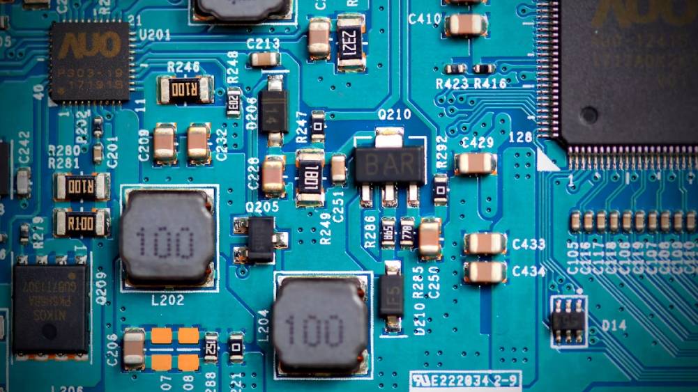
In modern electronics manufacturing, automated equipment – from pick‑and‑place machines to AOI systems and lithography steppers – relies on visual references to locate, align, and inspect components and circuits. These references are fiducial marks: deliberately placed, high‑contrast geometric patterns (typically circles, crosses, or squares) that provide a fixed coordinate system for machine vision.
Fiducial marks enable:
SMT placement – correcting for board expansion, rotation, and translation before component mounting.
AOI (Automated Optical Inspection) – aligning inspection algorithms to the actual board layout.
Multi‑layer registration – ensuring that successive layers in a build‑up process are precisely overlaid.
Wafer‑level packaging – guiding die attach, wire bonding, and moulding operations.
Traditionally, fiducials on PCBs were either etched copper pads (defined during circuit patterning) or screen‑printed ink dots. Both methods have drawbacks: etched copper can be obscured by solder mask or oxidation, and printed ink may lack durability or contrast after multiple thermal cycles.
Laser fiducial marking has emerged as the superior solution for a broad range of substrates – rigid and flexible PCBs, semiconductor packaging materials, glass panels, and ceramics. It is a mask‑less, dry, single‑step process that produces permanent, high‑contrast marks with micron‑level precision. (In the semiconductor wafer front‑end, photolithography remains the standard for nm‑scale alignment marks; the laser approach discussed here addresses the PCB, packaging, and precision substrate segments.)
This article provides a comprehensive technical guide to laser fiducial marking, covering laser selection, process optimisation, application scenarios, and best practices for reliable automated alignment.
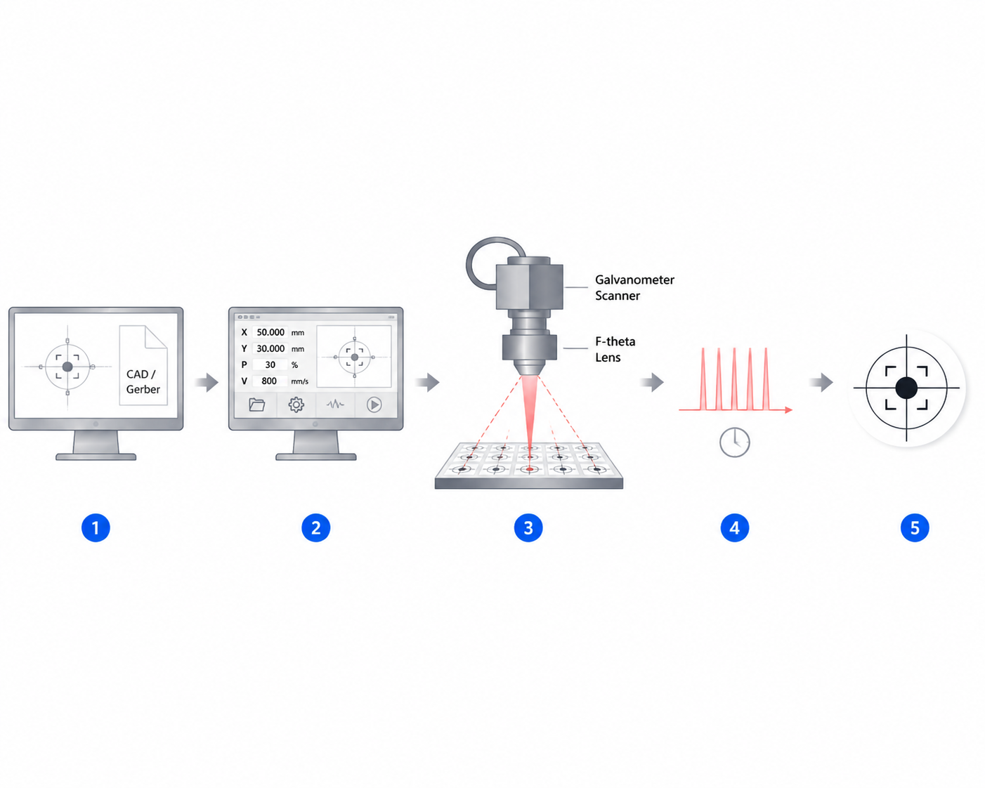
Laser fiducial marking works by directing a focused laser beam onto the substrate surface, modifying it to create a contrast difference visible to machine vision systems. The modification can be achieved through:
Ablation – removing a thin top layer (e.g., solder mask, oxide film, or coverlay) to expose an underlying material of different colour or reflectivity.
Surface texturing – creating a matte or roughened area on a glossy surface (e.g., polyimide coverlay) that scatters light differently.
Colour change – in some materials (metals, ceramics), laser heating can induce oxidation or phase transition, altering the surface colour.
The process is fully digital: no masks, no photoresist, no wet chemistry – just a clean, rapid, and reproducible operation.
The choice of laser wavelength and pulse duration determines the marking quality, substrate compatibility, and throughput. Two laser types dominate the field:
The UV nanosecond laser is the most widely adopted source for fiducial marking on PCBs, FPCs, solder mask, and coverlay. Its 355 nm wavelength is strongly absorbed by organic materials (polyimide, epoxy, solder mask) and copper, enabling efficient surface modification with minimal heat‑affected zone.
Preferred substrates:
Solder mask (all colours) – ablated to reveal a lighter base material.
Coverlay (polyimide) – surface texturing produces a matte, highly visible mark.
Copper pads – removal of surface oxide or light engraving.
FR4 and rigid laminates.
Advantages: High throughput, excellent contrast, proven reliability in high‑volume production, cost‑effective.
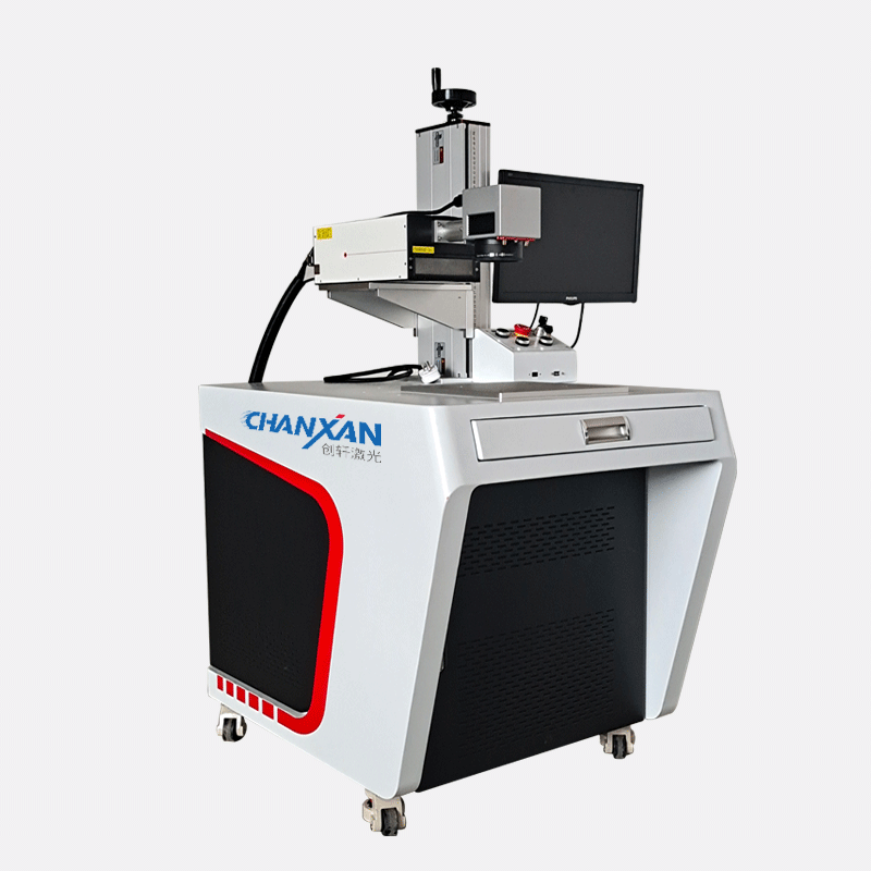
Chanxan offering: Chanxan UV Nanosecond Laser systems are production‑ready tools for PCB/FPC fiducial marking, widely used in SMT and AOI lines.
When the substrate is thermally sensitive – such as ultra‑thin glass, ceramic, low‑temperature co‑fired ceramic (LTCC), or advanced packaging films – a picosecond laser is the preferred choice. Its pulse duration below 10 ps removes material via cold ablation, virtually eliminating heat diffusion. This results in:
No carbonisation or burn marks.
No micro‑cracks or substrate stress.
Extremely sharp edges (linewidth down to 10–15 µm).
Consistent contrast even on transparent or highly reflective surfaces.
Preferred substrates:
Glass panels (display, photonics).
Ceramic substrates (LTCC, alumina).
IC packaging substrates (Ajinomoto build‑up film, polyimide tape).
High‑frequency laminates (LCP, PTFE).
Advantages: Zero thermal damage, ultra‑fine detail, suitable for contamination‑sensitive environments.
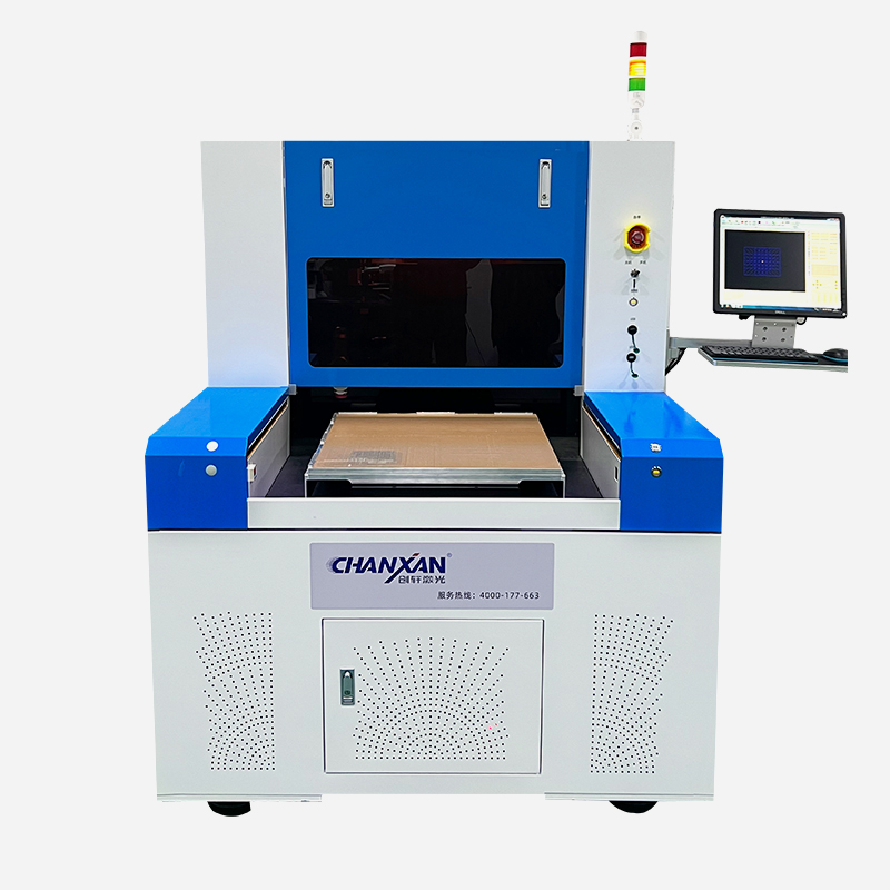
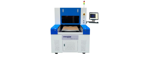
Chanxan offering: Chanxan CW‑6050PZ Picosecond Laser System is engineered for precision marking on glass, ceramic, and packaging substrates, delivering unsurpassed quality.
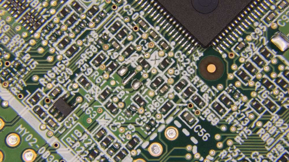
To produce marks that are consistently readable by vision systems, the following parameters must be carefully tuned:
| Parameter | Recommendation |
|---|---|
| Pulse energy | Start with the minimum energy that yields visible contrast. For solder mask: 0.5–2 µJ; for copper removal: 5–10 µJ. |
| Spot size | Typically 20–40 µm – larger spots give wider marks, smaller spots improve resolution. |
| Scan strategy | For circular marks, a single contour line often suffices; for filled marks, use a raster hatch with 50–70% overlap. |
| Number of passes | Usually one pass is enough – additional passes increase depth but are rarely required for fiducials. |
| Focus position | On‑surface focus for sharp edges; slight positive defocus (+0.5–1 mm) for softer, wider marks on coverlay. |
| Assist gas | Clean dry air or nitrogen at 1–2 bar removes debris and prevents oxidation (especially on copper). |
| Scan speed & repetition rate | Balance throughput and pulse overlap – ensure sufficient overlap for uniform marks (e.g., 50–70% along the line). |
Laser fiducial marking serves a wide range of industries and manufacturing stages:
| Application Area | Specific Use |
|---|---|
| PCB assembly | SMT placement fiducials; AOI reference points; flying‑probe test alignment. |
| FPC manufacturing | After coverlay lamination – marks that reflect final board geometry (capturing distortion). |
| Semiconductor packaging | IC substrates, interposers, lead frames – alignment for die attach, wire bonding, and encapsulation. |
| Display panels (glass) | Alignment for printing, cutting, and module assembly. |
| Ceramic / hybrid circuits | Screen‑print registration and component placement. |
| Multi‑layer rigid‑flex | Inner‑layer fiducials for X‑ray alignment before lamination. |
In FPC production, laser marking after lamination is particularly valuable because it accounts for panel shrinkage and distortion – a capability that pre‑etched copper marks cannot offer.
To ensure robust detection, design engineers should follow these recommendations:
| Design Parameter | Recommended Value / Practice |
|---|---|
| Shape | Solid circle or cross‑hair – circles are preferred for centroid‑based vision algorithms. |
| Diameter | 1.0–1.5 mm (standard); ≥0.5 mm for high‑magnification systems. |
| Clearance | Keep a ≥0.5 mm clear area around the mark (no copper, text, or vias). |
| Number of marks | Minimum 2 (3 recommended) to define translation, rotation, and scaling. |
| Placement | Near corners, at least 5 mm from board edges. |
| Contrast | Mark must have ≥30% grey‑level difference from background under the vision illumination. |
| Surface condition | For copper marks, ensure they are not covered by solder mask – laser can ablate the mask to expose copper. |
| Panel fiducials | For panel‑based assembly, add extra marks at panel level for global alignment. |
Even with optimised parameters, defects can occur. The table below lists typical issues and corrective actions:
| Defect | Visual Sign / Detection Failure | Root Cause | Solution |
|---|---|---|---|
| Low contrast | Mark blends with background; camera cannot locate | Insufficient pulse energy; wrong focus; unsuitable scanning strategy | Increase energy; re‑focus; adjust hatch pattern; try a different scan mode. |
| Carbonised / burnt edges | Dark halos or spatter around mark | Excessive energy or heat accumulation | Reduce pulse energy; increase scan speed; use nitrogen assist; switch to picosecond if persistent. |
| Incomplete or uneven mark | Broken or non‑uniform lines | Dirty optics; power instability; insufficient pulse overlap | Clean optics; verify laser power; increase repetition rate or reduce speed. |
| Mark too deep | Copper fully removed exposing dielectric; risk of electrical damage | Over‑ablation (too many passes or too high energy) | Reduce number of passes; lower fluence; use surface texturing instead of engraving. |
| Misplaced mark | Mark shifts from nominal position | Panel distortion; galvo calibration drift | Use local fiducial compensation; re‑calibrate scanner; apply distortion correction. |
| Mark disappears | Mark fades or is covered by flux residue after soldering | Mark on surface coating only (e.g., ink) | Use laser ablation to reach a permanent layer (copper or base material). |
Recommended inspection: After marking, verify each fiducial using an AOI system – check size, roundness, and contrast. A deviation of >10% from nominal warrants parameter adjustment.
Fiducial marks are small features with a big impact. They are the foundation upon which automated assembly, inspection, and multi‑layer registration are built. Laser fiducial marking provides the most versatile, durable, and precise method for creating these critical references across a wide range of substrates – PCBs, FPCs, packaging materials, glass, and ceramics.
Key advantages of laser marking:
Mask‑less and digital – instant design changes, no tooling cost.
Permanent and durable – marks survive soldering, cleaning, and handling.
High contrast – optimised for machine vision under various lighting conditions.
Substrate‑versatile – works on solder mask, copper, polyimide, glass, ceramic, and more.
Integratable – can be combined with drilling, skiving, and trimming on a single platform.
The choice of laser source depends on the application:
UV nanosecond – the workhorse for PCBs and FPCs, balancing speed, cost, and quality.
UV picosecond – the premium option for delicate substrates (thin glass, ceramic, packaging films), offering cold ablation with zero carbonisation and ultra‑fine resolution.
Chanxan offers a comprehensive product line to address both needs:
Chanxan UV Nanosecond Laser systems are proven production tools for high‑volume PCB and FPC fiducial marking, delivering reliable contrast and throughput in SMT and AOI environments.
Chanxan Picosecond Laser System is the premier solution for high‑end packaging, glass, and ceramic applications, where precision and substrate integrity are paramount. Its cold ablation process ensures marks free from thermal artefacts, meeting the most stringent quality requirements. With Chanxan, manufacturers gain a flexible, precise, and production‑ready solution for all their fiducial marking needs – from rapid prototyping to high‑volume manufacturing.
| Free solution