Key Words: Silicon Wafer Dicing PCB Depaneling Glass Cutting
Home > News > Industry News
【Description】:
Discover advanced flexible PCB laser processing solutions for TPU, PEEK & ETFE polymers. Eliminate carbonization & thermal distortion with Chanxan ultrafast systems.
In advanced flexible PCB laser processing, material selection plays a decisive role in determining cutting quality, process stability, and final device reliability. Among emerging engineering polymers, TPU (Thermoplastic Polyurethane), PEEK (Polyether Ether Ketone), and ETFE (Ethylene Tetrafluoroethylene) are increasingly used in high-performance flexible electronic systems.
These materials are not conventional substrates like PET or PI. They are designed for demanding environments, which also means they respond very differently during laser cutting. Understanding their behavior is essential for achieving stable and high-quality microfabrication results.
TPU is widely used in flexible PCB assemblies as a protective encapsulation layer, shock-absorbing film, or flexible insulating structure. Its elasticity and softness make it suitable for wearable electronics and dynamic bending applications.
Edge deformation caused by localized overheating.
Material shrinkage and dimensional recovery after cutting.
Inconsistent ablation rates depending on specific TPU formulations.
High elasticity and deformation recovery; low melting point compared to engineering plastics; strong thermal sensitivity under continuous exposure.
Low thermal load processing is strictly required to prevent edge melting; short pulse duration helps drastically minimize thermal diffusion.
PEEK is a high-performance thermoplastic widely used in aerospace-grade flexible circuits, medical electronics, and high-temperature resistant electronic assemblies. It provides excellent mechanical strength and chemical resistance but is one of the most challenging polymers to process.
Severe carbonization at cutting edges under improper energy settings.
Uneven absorption patterns driven by highly crystalline structures.
Significantly higher ablation threshold compared to PI or PET standard matrices.
Extremely high melting temperature (~343°C); peak crystallinity and structural stability; strong resistance to chemical or thermal breakdown.
High peak power with ultrashort pulse duration is mandatory; precise energy density control is critical to avoid edge carbonization pathways.
ETFE is widely used in high-frequency flexible circuits, harsh-environment insulation systems, and aerospace electronics due to its excellent dielectric properties and chemical resistance.
Edge shrinkage due to back-end thermal accumulation.
Extremely limited photon absorption efficiency at standard laser wavelengths.
Difficulty achieving high precision without deep laser parameter optimization.
Low surface energy and low baseline laser absorption; high chemical and UV resistance; exceptionally stable dielectric performance under extreme environments.
Requires highly optimized wavelength selection for efficient photon coupling; high pulse energy with structured precision scanning paths is critical.
| Material | Core Processing Challenges & Behaviors | Engineering Control Mandates |
|---|---|---|
| TPU | Easy to deform, melt, and contract along cut boundary. | Requires ultra-low thermal load metrics and strictly calibrated pulse gating. |
| PEEK | High-temperature resistant, heavily prone to conductive carbonization rings. | Demands high peak power ultrafast precision micro-ablation over multiple passes. |
| ETFE | Chemically ultra-stable but exhibits highly transparent, low-absorption behavior. | Requires highly optimized wavelength matching paired with targeted fast-scanning tactics. |
When TPU, PEEK, and ETFE are integrated into flexible PCB structures, they are usually combined with copper circuits, adhesive layers, and insulating films. This multi-layer structure introduces additional processing challenges:
Material stacking leads to highly inconsistent internal thermal responses.
Different absorption rates require adaptive, real-time laser parameter control.
Edge quality must be perfectly maintained across entirely heterogeneous layers.
Dimensional accuracy remains critical for micro-scale functional electronic assemblies.
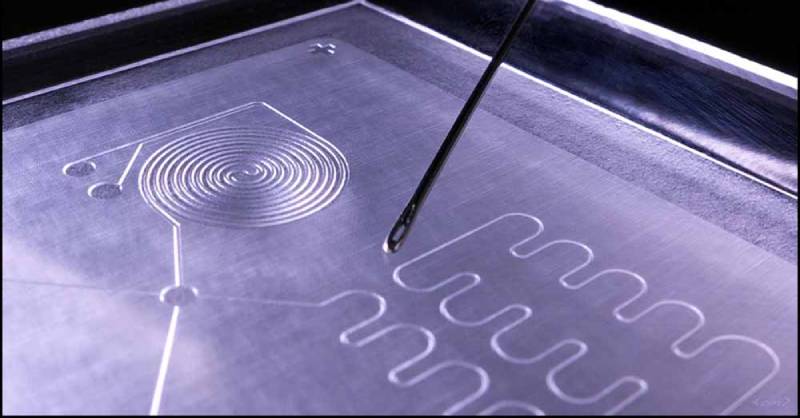
To address the processing challenges of TPU, PEEK, and ETFE in flexible PCB laser processing, Chanxan provides advanced ultrafast laser systems designed for high-precision industrial applications.
The Chanxan picosecond and UV laser platforms are engineered to deliver controlled energy deposition with minimal thermal diffusion, making them suitable for complex polymer structures and multilayer flexible electronic materials.

TPU, PEEK, and ETFE represent three important classes of advanced flexible materials used in modern electronics. Each material presents unique challenges in laser processing, from thermal deformation in TPU to high crystallinity in PEEK and low absorption in ETFE.
Successful flexible PCB laser processing requires not only selecting the correct laser source but also optimizing process parameters according to material behavior. With proper system configuration, high-quality, stable, and scalable production can be achieved across these advanced polymers.
| Free solution
Previous: PEN (Polyethylene Naphthalate)
Next: Flexible PCB Laser Processing Solutions: A Complete Guide to Materials, Methods, and Applications