Key Words: Silicon Wafer Dicing PCB Depaneling Glass Cutting
Home > News > Industry News
【Description】:
Discover PEN film laser cutting solutions for flex PCB manufacturing, including circuit profiling, coverlay opening, and precision feature processing. Chanxan CO2 and picosecond laser systems support clean, efficient PEN processing for flexible electronics production.
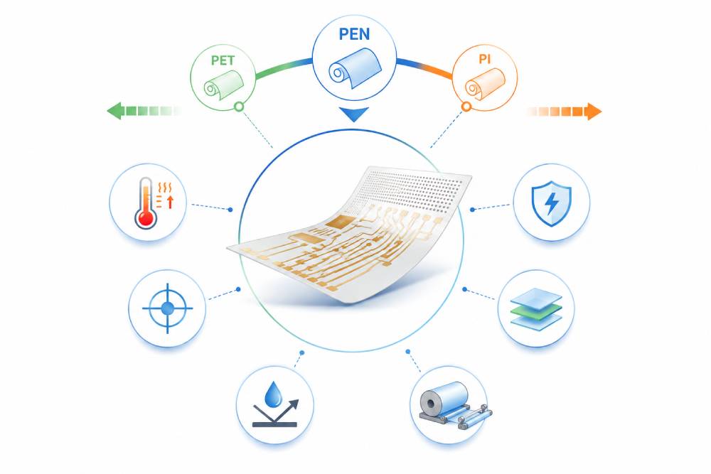
In the flexible electronics supply chain, PEN occupies an important middle ground between PET and polyimide.
PET remains attractive for low-cost flexible circuits, labels, and membrane switches, but its low temperature resistance limits its performance during demanding SMT reflow or assembly steps. Conversely, Polyimide (PI) serves as the high-reliability benchmark, though its elevated material cost can be restrictive. PEN is selected when engineers demand a substrate that performs more robustly than PET under thermal stress without stepping up to the expense of a full PI stack.
For flex PCB and printed electronics manufacturers, PEN provides several key advantages:
Higher Thermal Stability: More tolerant of elevated processing and soldering temperatures than standard PET.
Superior Dimensional Stability: Critical for keeping copper traces, printed conductive inks, and laminated coverlays in perfect registration.
Low Moisture Absorption: Improves dielectric consistency and prevents process drift in high-humidity operating environments.
Excellent Dielectric Behavior: Well-suited for printed sensors, high-density LED circuits, and low-to-mid-frequency flexible structures.
Roll-to-Roll Compatibility: Highly adapted to continuous web handling, printing, and continuous laser singulation.
While PEN improves heavily on PET, from a laser processing standpoint, it remains a thermoplastic polyester. This classification completely shifts how the material responds to heat compared to standard thermoset materials like Polyimide.
When a laser beam strikes PEN, the target is clean sublimation/ablation. If energy density is too low or dwell time is too long, heat conducts into the surrounding polymer matrix. Instead of clean removal, the film softens, flows, and re-solidifies into a prominent, raised edge bead—a critical defect in precision electronics fabrication.
Melt-rounded cut profiles that disrupt flat mechanical fitment or downstream lamination.
Local edge-bead accumulation that degrades coverlay adhesion and induces delamination.
Dimensional shrink-back on narrow internal cut paths and circuit windows.
Heat-induced registration drift that disrupts precise downstream pick-and-place (SMT) routines.
Edge carbonization (charring) or polymer yellowing under excessive dwell times.
| PEN Processing Task | Typical Laser Operation | Common Examples | Recommended Laser Architecture |
|---|---|---|---|
| Flex Circuit Outline Profiling | Outer contour cutting and singulation after etching or lamination. | Circuit boundaries, connector tongues, mounting tabs. | RF CO2 Laser (High throughput) |
| Coverlay & Adhesive Windows | Selective removal of cover films to expose conductor pads. | Coverlay openings, pad access slots, alignment holes. | CO2 or Picosecond (Based on copper proximity) |
| Micro-Slotting & Apertures | Cutting intricate vents and slots within internal layers. | Sensor vents, acoustic openings, sub-millimeter slots. | Picosecond Laser (Ultra-low HAZ / Tighter tolerances) |
| Roll-to-Roll Singulation | High-speed web cutting of continuous printed electronic sheets. | Printed heaters, biosensor strips, smart RFID labels. | RF CO2 Laser (Scalable web speed) |
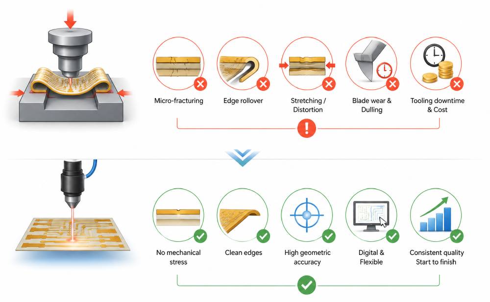
While hard tooling or die cutting appears viable due to PEN's rigidity, mechanical stress introduces extensive micro-fracturing along delicate copper-backed interfaces. Die-stamping causes edge rollover on thin films and relies on physical clamping forces that can permanently stretch or distort flexible circuits. Furthermore, physical blades gradually dull over time, introducing unpredictable quality degradation and requiring expensive tooling downtime whenever part geometry changes.
Laser processing introduces a completely non-contact, digital solution. It bypasses physical stress entirely, guaranteeing consistent geometric accuracy from the first part to the last.
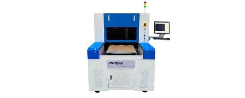
Industrial processing of PEN flex boards splits into two main machine pathways based on throughput requirements and feature density.
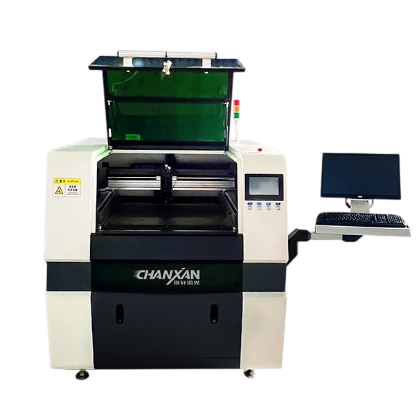
Operating at 10.6 μm, RF CO2 lasers are heavily absorbed by organic polyester chains, making them highly economical for contour profiling, perimeter cutting, and high-volume web processing. They are the ideal choice for bulk material removal where cutting speed and capital equipment ROI take precedence over micron-level edge limits.
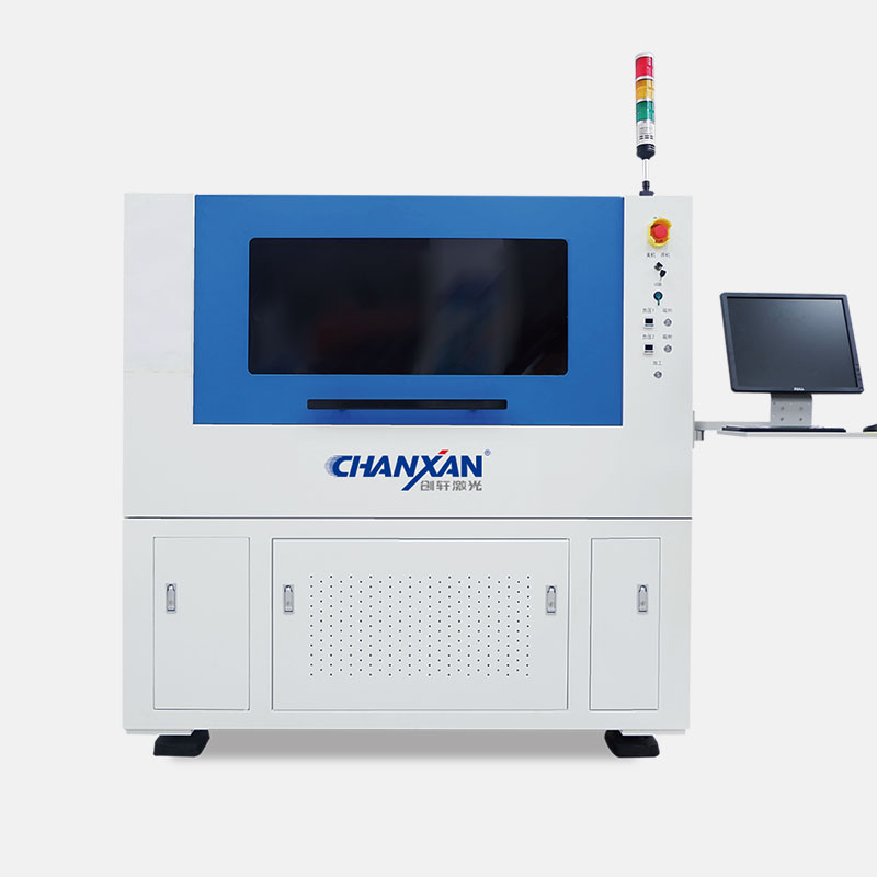
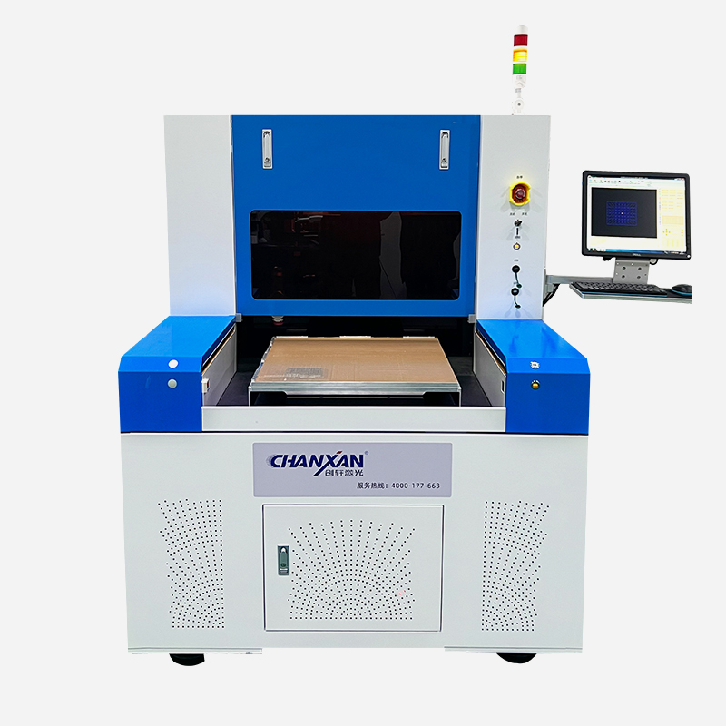
When cutting features directly adjacent to fine copper traces, a picosecond laser is indispensable. By delivering ultra-short pulses measured in trillionths of a second, the material is vaporized instantaneously via localized "cold ablation" before significant thermal energy can conduct into the adjacent matrix. This eliminates edge beads, keeps coverlay window geometries razor-sharp, and preserves adhesive bond lines.
| Processing Requirement | RF CO₂ Laser System | Picosecond Laser System |
|---|---|---|
| Bulk PEN Outline Cutting | Excellent (Highest throughput) | Good (Lower throughput) |
| Fine Windows near Copper Traces | Moderate (Risk of thermal margin loss) | Excellent (No copper damage) |
| Minimal Heat Affected Zone (HAZ) | Moderate | Excellent (Sub-micron thermal control) |
| Micro-Features & Narrow Slots | Limited by focal spot size | Excellent (High aspect ratio cuts) |
| Capital Investment Efficiency | Highest ROI per throughput | Higher entry cost / Premium performance |
Avoid registration drift, tool wear, and deformed edge beads by moving to ChanXan's digital laser processing platforms. Let our application lab determine the optimal wavelength and pulse duration for your specific PEN laminate stack.
| Free solution
Previous: Burr Formation in Flexible PCB Laser Cutting: Causes and Solutions
Next: Flexible PCB Laser Processing Solutions: A Complete Guide to Materials, Methods, and Applications