Key Words: Silicon Wafer Dicing PCB Depaneling Glass Cutting
Home > News > Industry News
【Description】:
Selective, substrate-safe removal of conformal coating, solder mask, and encapsulant for rework, test-point access, and failure analysis — without abrasion, solvents, or collateral damage to copper.
TL;DR
Laser ablation removes coatings by exploiting the fluence gap between the coating's ablation threshold and copper's much higher threshold — the process self-limits at the metal surface.
Picosecond and femtosecond (ultrafast) lasers deliver that energy faster than heat can diffuse into the laminate — this is cold ablation: minimal heat-affected zone, no charring, no undercut.
Coatings on a PCB do two jobs at once: they protect the board, and they get in the way the moment someone needs to reach what's underneath. A rework technician needs to expose a failed component's pads. A test engineer needs a bare-copper probe point. A production line needs to open an RF grounding window on ten thousand boards, with the same boundary every time. Whatever the conformal coating, solder mask, or potting compound is protecting against, it is now standing between the operator and the copper — and this is exactly the problem laser ablation was built to solve.
This page covers what's actually being removed, why mechanical and chemical methods struggle to keep up with modern board density, the physics that make selective laser ablation possible, and why ultrafast — picosecond and femtosecond — sources outperform CO2 and nanosecond lasers for this specific job.
Conformal coating chemistry is organized around five families defined in IPC-CC-830: acrylic (AR), polyurethane (UR), silicone (SR), epoxy (ER), and parylene (XY). Each trades off protection, flexibility, and rework-friendliness differently — and each behaves differently under a laser beam. Solder mask (typically a UV-cured, epoxy-acrylate liquid photoimageable formulation) and potting or encapsulant compounds round out the materials that get selectively opened rather than fully recoated.
| Coating Chemistry | Typical Thickness | Behavior Under Laser Ablation |
| Acrylic (AR) Acrylic resin | ~25–130 µm | Low ablation threshold; clean vaporization, minimal residue. |
| Polyurethane (UR) Urethane resin | ~25–75 µm | Moderate threshold; can char if fluence overshoots with longer pulses. |
| Silicone (SR) Silicone resin | ~50–200 µm | Flexible; thermally driven decomposition leaves silica residue — short pulses reduce this. |
| Epoxy (ER) Epoxy resin | ~30–130 µm | Rigid; threshold margin to copper is narrower, benefits from tight fluence control. |
| Parylene (XY) CVD parylene C/N | ~5–50 µm | Solvent-inert — laser is the dominant removal route; low-fluence lift-off possible on thin films. |
| Solder mask (LPISM) UV-cured epoxy-acrylate | ~15–40 µm | Strong absorption near 355 nm; same family as ER, well-characterized ablation window. |
| Potting / encapsulant Filled epoxy or silicone | ~0.5–5 mm | Bulk removal needs a multi-pass strategy, not single-shot ablation. |
Thickness ranges are typical industry figures and vary by formulation, application method, and board design — treat as planning estimates, not specification values.
Mechanical removal — glass-fiber pens, micro-abrasion, hand scraping — depends on a steady hand and a forgiving pitch. At fine-pitch geometry, it's easy to gouge a trace or lift a pad, and results vary across operators and shifts in a way that's hard to qualify for production use.
Chemical stripping dissolves coatings selectively, but generates waste that needs licensed disposal, demands PPE and ventilation, and is largely ineffective against chemically inert coatings like parylene. It can also attack adjacent components, adhesives, or markings that were never meant to be stripped.
Neither method offers reliable depth control that stops precisely at the copper surface, and neither scales to a rework cell where the same opening boundary has to land in the same place, board after board.
Why this matters at scale: a method that's "close enough" on a one-off repair becomes a yield problem the moment it has to run on a production line opening the same RF grounding window or test point on every board.
Every material has an ablation threshold — a minimum energy density per unit area (fluence, measured in J/cm²) needed to break molecular bonds and eject material. Organic coating polymers absorb strongly at common processing wavelengths, particularly near-UV (around 355 nm couples efficiently with C–C, C–O, and C–H bonds), and ablate at comparatively low fluence. Copper, by contrast, is far more reflective at those wavelengths and carries a much higher ablation threshold. Operating in the window between "removes the coating" and "starts removing copper" makes the process self-limiting — the system doesn't need to know coating thickness with perfect precision, because the ablation naturally stalls once it reaches the more energy-resistant metal.
For thin films — parylene being the clearest example — a second mechanism is available at low fluence: the beam transmits through the thin coating with little absorption, couples into a thin interface layer beneath it, and the resulting localized stress mechanically delaminates the film above with minimal thermal load on the bulk substrate. This laser lift-off effect gives way to direct photothermal ablation as fluence increases.
Pulse duration changes which of these mechanisms dominates. At picosecond and femtosecond pulse widths, peak intensity is high enough that multiphoton absorption becomes significant — even partially transparent or weakly absorbing layers can be processed through non-linear absorption rather than relying purely on linear photothermal coupling. That widens the set of coatings the process can address selectively, and it's the same physical reason ultrafast sources run measurably "colder" than their longer-pulse counterparts.
Pulse duration decides how much absorbed energy turns into heat that spreads into the substrate, versus energy that goes directly into breaking bonds and ejecting material. The shorter the pulse, the less time heat has to diffuse before the material is already gone.
| Laser Class | Typical Pulse Duration | Dominant Mechanism | HAZ / Char Risk | Best Fit |
| CO2 | Continuous / long-pulse (µs+) | Thermal melting & vaporization | High — strong coupling with organics, heat spreads broadly | Bulk coating stripping where fine boundary control isn't critical |
| Nanosecond UV | ~1–200 ns | Photothermal, some photochemical | Moderate — usable, but margin to copper is narrow | General-purpose mask opening, cost-sensitive lines |
| Picosecond | ~1–50 ps | Photochemical-dominant, low thermal diffusion | Low — measurably less HAZ and edge haze than nanosecond | Fine-pitch rework, RF/EMI windows, repeatable production opening |
| Femtosecond | <1 ps | Multiphoton / non-linear, near-athermal | Minimal — energy deposited faster than thermal diffusion time | Most sensitive substrates, failure-analysis-grade precision |
Published comparisons of picosecond- and nanosecond-ablated metallic-coating edges on the same substrate show visibly less haze and a smaller heat-affected zone with the picosecond source, because the pulse delivers its energy faster than the surrounding material can conduct heat away. Paired with linear-motor stages and CCD vision alignment, that translates into the kind of micron-level, repeatable boundary control that fine-pitch boards and production rework cells actually need.
Open a precise window around a failed component before resoldering, without lifting coating on neighboring parts or marring adjacent pads.
Remove solder mask to expose bare-copper probe points and test pads for in-circuit test, without breaking trace continuity.
Open a clean copper window for shield-can soldering or RF ground connections, where contact resistance depends on an undamaged surface.
Expose a trace or die-attach area for microscopy without introducing new artifacts that could be mistaken for the original failure.
Selective coating removal lives or dies on three things: a fluence window narrow enough to stop at copper, a pulse short enough to keep that window from collapsing into heat, and a stage and vision system precise enough to hold the boundary across thousands of boards.
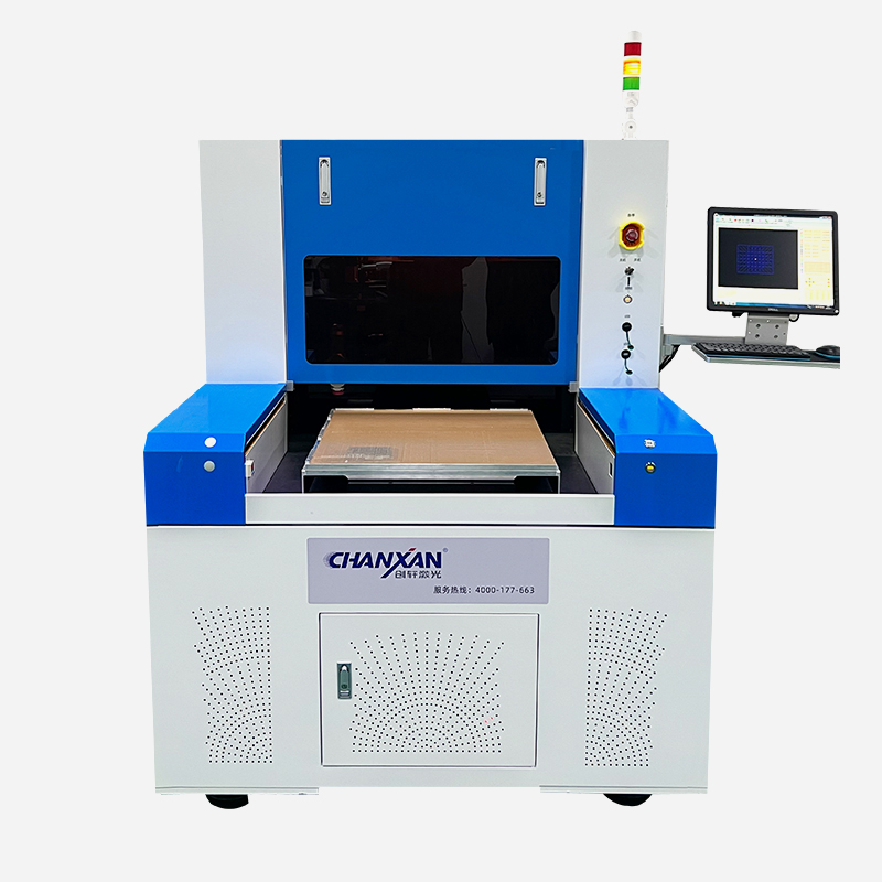
Chanxan's picosecond laser platform is engineered precisely around these requirements. With ultrashort pulse durations in the picosecond range, the system delivers highly controlled ablation of conformal coatings, solder mask, and other thin functional layers while minimizing thermal diffusion into the underlying copper circuitry. Its stable pulse energy and tightly managed fluence output create a repeatable processing window for selective layer removal without over-etching or substrate damage. Combined with high-precision motion control, machine vision alignment, and recipe-based automation, the platform can maintain clean coating-to-copper boundaries across large panel formats and high-volume PCB batches. The result is a reliable solution for selective coating removal, circuit repair preparation, and fine-feature PCB rework where consistency, edge quality, and copper protection are critical.
| Free solution
Previous: PTFE Laser Cutting & Microvia Drilling | CO2 and Picosecond Laser Solutions
Next: Precision Laser Direct-Write (LDW) for ITO Film Patterning