Key Words: Silicon Wafer Dicing PCB Depaneling Glass Cutting
Home > News > Industry News
【Description】:
Precision cutting and via drilling for PTFE and PTFE-based RF laminates, built around the one fact that makes this material different from almost everything else in this series: pure PTFE barely absorbs UV light at all.
PTFE's chemical inertness and near-zero dielectric loss are exactly why it ends up in RF and microwave PCB laminates, gaskets, seals, and cable insulation — and exactly why it resists most conventional processing methods. It barely bonds to adhesives, barely reacts with solvents, and mechanically it's soft enough to smear and deform under a blade rather than shear cleanly.
Laser processing looks like the obvious answer, except PTFE doesn't behave like most polymers in front of a beam. Depending on wavelength, it can be almost invisible to the light — which is the starting point for everything below, including which of ChanXan's two relevant machines actually fits a given PTFE job.
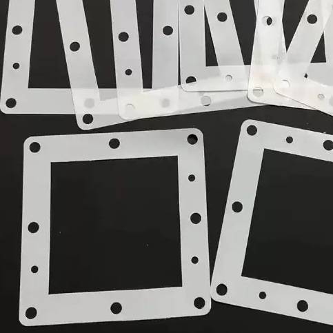
Most polymer ablation work relies on a material absorbing strongly at a UV wavelength. PTFE breaks that assumption. RF PCB fabricators report it directly: pure PTFE is UV-transparent, so a 355 nm beam passes through it without converting much energy into heat, making UV ablation largely ineffective on its own.
Ceramic-filled PTFE composites — used in many real RF laminates for added stiffness and thermal conductivity — add a second complication: the filler reflects the beam, which can make ablation inconsistent across a single feature depending on where the beam lands relative to filler particles.
CO2 lasers, operating at 10.6 µm in the mid-infrared, sit on a band PTFE does absorb. That's why CO2 has long been the practical default for PTFE sheet cutting and for via drilling on RF laminates, where reported microvia diameters commonly fall in the 50–100 µm range.
Picosecond and femtosecond pulses don't depend on the same linear absorption a CO2 or UV-nanosecond source needs. At the peak intensities a sub-nanosecond pulse reaches, energy can couple into the material through multiphoton (nonlinear) absorption — a mechanism that doesn't require the beam's wavelength to sit on one of the material's native absorption bands.
That's the same physical principle that lets femtosecond lasers machine optically transparent materials like glass and sapphire, and it's why ultrafast sources can process PTFE cleanly even though the material is, by design, doing its best to ignore a UV beam. In practice, that supports finer microvias and antenna-pattern trims on RF laminate with less of the melt-rounded edge and discoloration that longer-pulse processing can leave.
| Laser Type | Wavelength / Pulse | Absorption in PTFE | Typical Role | Trade-off |
|---|---|---|---|---|
| CO2 | 10.6 µm, long-pulse/CW | Strong (mid-IR) | Bulk sheet cutting; established RF-laminate via drilling | Wider HAZ, melt-rounded edges, higher fume volume per cut |
| UV Nanosecond | 355 nm, ~1–200 ns | Weak — largely passes through unfilled PTFE | Limited; mainly filled/composite or pre-treated surfaces | Unreliable as a default on unfilled PTFE |
| Picosecond / Femtosecond | <50 ps / <1 ps | Nonlinear (multiphoton) — independent of native absorption | Fine microvias, antenna trim, precision features | Higher equipment cost; lower throughput than CO2 on thick bulk sheet |
RF / Microwave: Drilling fine interlayer vias on PTFE and ceramic-filled PTFE laminates for phased-array and mmWave modules.
Precision Trim: Defining or trimming copper antenna geometry on PTFE substrate without melt-flow into the surrounding dielectric.
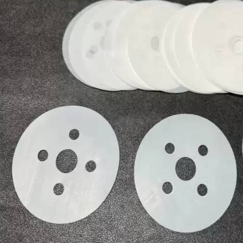
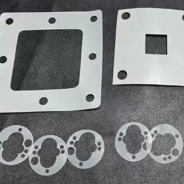
Industrial: Profile-cutting PTFE sheet for chemical-resistant gaskets and seals — typically a CO2 task at production scale.
Cable Assembly: Trimming PTFE-insulated wire and connector components where clean, non-deformed edges matter.
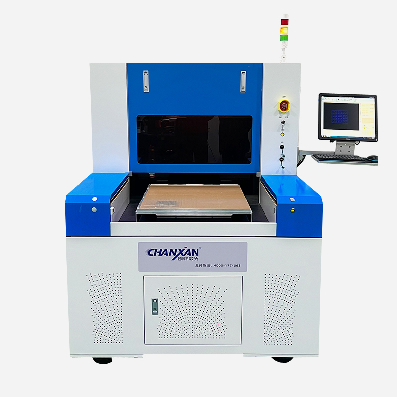
PTFE genuinely splits into two equipment categories, and ChanXan manufactures the high-performance digital machine for each side of that split.
For bulk PTFE sheet and film cutting — gaskets, seals, insulation, and general film-type material processing — ChanXan's High-Precision RF CO2 Laser Non-Metal Cutting Machine is built specifically for this category, powered by an imported hermetic CO2 RF-tube source.
| Features & Specifications | Parameters |
|---|---|
| Model | CW-650R |
| Laser Type | Imported CO2 Hermetic RF Tube |
| Laser Power | 30W - 150W (Optional) |
| Working Area | 600 x 500mm |
| Positioning Accuracy | ±0.01mm |
| Cutting Speed | 0 - 40000mm/min |
| Engraving Speed | 0 - 60000mm/min |
| Maximum Moving Speed | 1000mm/s |
| Drive System | Imported Servo Motor System |
| Control Software | DSP Control System |
| Supported Formats | DXF, PLT, BMP, AI, HML, DST |
| Cooling System | Water / Air Cooling Protection System |
| Working Environment | Temperature: 1°C - 45°C | Humidity: 5% - 95% |
| Power Requirement | AC 220V ±10%, 50Hz / 60Hz |
For the fine-feature side — RF laminate microvias, antenna pattern trimming — ChanXan's Picosecond Laser System is the ideal industrial tool, leveraging the nonlinear multiphoton absorption mechanism detailed above to maximize microvia precision.
| Features & Specifications | Parameters |
|---|---|
| Model | CW-6050PZ |
| Laser Type | Picosecond UV / IR / Green |
| Laser Power | 30W |
| Transmission System | X / Y / Z Three Axis |
| Working Area | 500*500mm / 600*900mm |
| Adsorption Platform Size | 1200mm*700mm (Customized) |
| Machining Thickness | <= 3mm |
| Machining Speed | 3000mm/s |
| Overall Machining Accuracy | 30um |
| Positioning Accuracy | 1um |
| Repeatability | 1um |
| Software Control System | Chanxan Self-developed Suite |
| Supported Formats | PLT, BMP, DXF, DWG, AI, LAS, etc. |
| Overall Dimension | 2100mm*1550mm*1750mm |
| Supply Voltage | 380V ±10%, 50HZ |
Whether you need high-speed CO2 cutting for bulk PTFE sheets or ultra-precision picosecond machining for RF microvias, ChanXan provides tailored laser solutions for your material requirements. Contact our engineering team today for custom testing and quotes.
| Free solution
Previous: Flexible PCB Laser Processing Solutions: A Complete Guide to Materials, Methods, and Applications
Next: Selective PCB Coating Removal: Precision Laser Rework & FA