Key Words: Silicon Wafer Dicing PCB Depaneling Glass Cutting
Home > News > Industry News
【Description】:
Selective removal of a transparent conductive layer that's often thinner than the wavelength of light used to remove it — without scarring the glass, PET, or PI underneath.
Indium tin oxide (ITO) does one job, transparently: it conducts electricity through a layer thin enough to barely register as a layer at all. That thinness is the whole appeal, and the whole processing problem. A touch sensor needs that ITO layer cut into isolated electrodes; a thin-film solar cell needs it scribed into separated interconnect strips; an OLED backplane needs it patterned into individual pixel electrodes.
All of it has to happen without disturbing the glass, PET, or polyimide carrying the film, and without leaving conductive debris at the cut edge that bridges two electrodes meant to stay isolated.
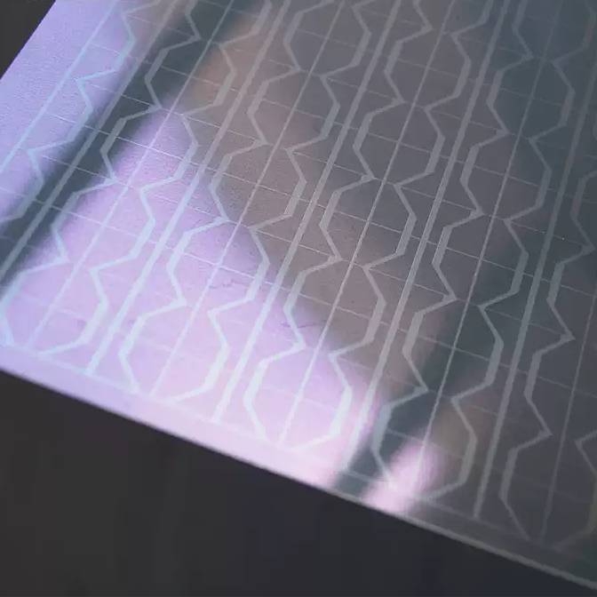
Data shows that the "ablation threshold" of ITO (the minimum laser energy required to remove it) is vastly lower than that of the underlying substrate.
Against Glass Substrates: Stripping ITO requires only about 0.07 J/cm² of energy, whereas damaging the glass underneath requires a massive 1.2–1.6 J/cm².
Against PET Plastic Substrates: Even for less heat-resistant PET, its damage threshold (around 0.56 J/cm²) is still several times higher than that of ITO.
This near "order-of-magnitude" safety margin is much wider than the typical gap found in PCB coating removal. This huge tolerance window is exactly why Laser Direct-Write (LDW) has successfully replaced traditional wet chemical etching in high-precision manufacturing, such as the front-electrode patterning step for thin-film solar cells.
How it works is quite simple: The removal mechanism depends on the laser's photon energy relative to ITO's bandgap:
When energy is below the bandgap, the laser acts like an "invisible bulldozer," heating the ITO up and forcing it to melt and flow away.
When energy is above the bandgap, it acts like an "instant vaporizer," directly blasting the ITO material away through vaporization.
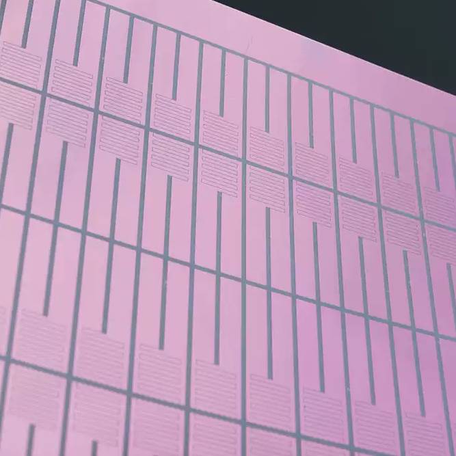
Even with a comfortable fluence window, nanosecond ITO scribing has a well-documented failure mode: melt-driven removal pushes material sideways and leaves raised ridges at the groove rim, sometimes tens of nanometers tall, which can act as stray conductive bridges at fine pitch.
Picosecond pulses, working faster than the melt has time to flow, produce visibly smoother groove bottoms and substantially smaller rim ridges on the same film. Comparative studies across 355, 532, and 1064 nm picosecond pulses found 1064 nm front-side irradiation gave the cleanest result — a smooth groove bottom, near-vanishing rim ridges, and a heat-affected zone too small to register — while 532 nm showed measurably weaker absorption and correspondingly lower scribing quality.
| Laser / Wavelength | Typical Use | Edge Quality | Substrate Risk | Notes |
|---|---|---|---|---|
| Nanosecond, 532/1064 nm | Cost-driven scribing; thin-film PV front contact | Moderate — visible rim ridges from melt flow | Low–moderate | Already standard replacement for wet etch in several processes |
| Picosecond, 532 nm | General-purpose patterning | Limited by weaker ITO absorption | Low | Quality more sensitive to fluence control |
| Picosecond, 1064 nm | Fine-pitch touch sensor, OLED pixel definition | High — smooth groove, near-vanishing ridges | Negligible HAZ reported | Generally the strongest published result for this film |
| Femtosecond | R&D, ultra-fine pitch, sensitive flexible substrate | Highest — minimal thermal contribution | Lowest | Throughput/cost trade-off versus picosecond |
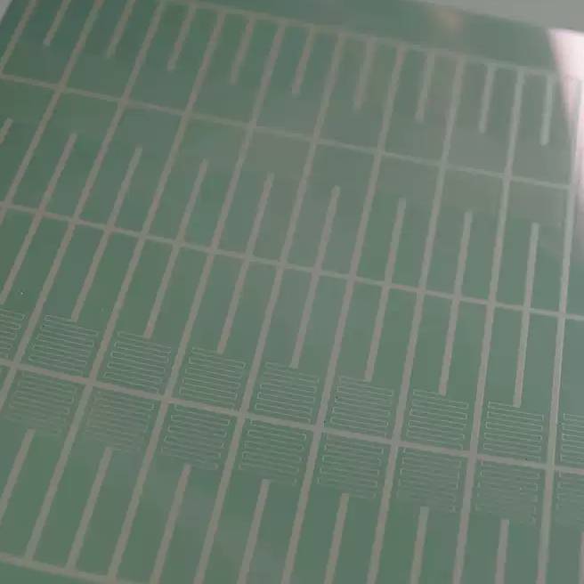
Capacitive Touch: scribing isolation lines between ITO electrodes at fine pitch without bridging or substrate cracking.
Display Backplane: patterning ITO pixel electrodes with clean, repeatable edges across large-area substrates.
Photovoltaic: front-contact scribing on the ITO layer, the process that has already displaced wet etch in much of this segment.
Functional Film: patterning conductive circuits into ITO-coated heater and shielding films on flexible substrate.
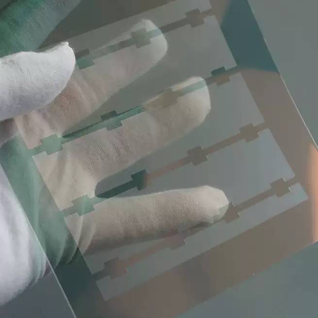
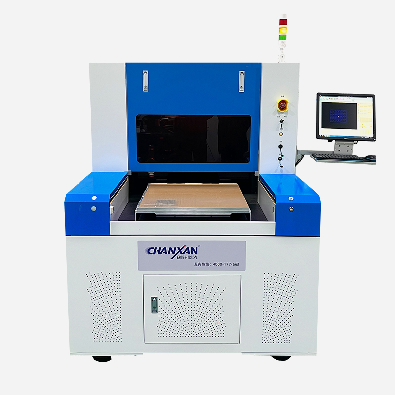
ITO patterning rewards exactly what a vision-aligned ultrafast system is built for: a wide, forgiving fluence window, a pulse short enough to avoid melt-driven rim ridges, and registration tight enough to land isolation lines precisely. To fully leverage this material advantage, we recommend our Industrial Picosecond Laser Series, engineered specifically for high-yield ITO and fluoropolymer processing.
The 1064 nm Advantage: Delivers the exact infrared wavelength recommended by industry studies to maximize the ablation threshold gap between the ITO film and glass or PET substrates.
Cold Processing via Picosecond Pulses: With pulse widths measured in trillionths of a second, the laser vaporizes the ITO film instantly before heat can transfer to neighboring areas, eliminating micro-cracking and melted ridges.
Order-of-Magnitude Safety Margin: The system's precise power modulation allows you to lock into the exact window (e.g., 0.07 J/cm²) needed to cleanly eject the ITO layer while remaining safely below the damage threshold of delicate backing materials.
Flexible Configuration: The same base platform can be dynamically configured with standard or high-power 1064 nm IR sources, allowing you to easily scale from prototype testing to 24/7 high-throughput solar cell or touch-panel production lines.
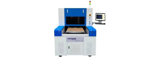
Contact Chanxan Laser’s engineering team today for custom sample testing, process parameters evaluation, and tailored picosecond laser equipment solutions.
Get a Free Consultation & Sample Testing| Free solution
Previous: Selective PCB Coating Removal: Precision Laser Rework & FA
Next: LCP Laser Processing & Microvia Drilling for 5G mmWave