Key Words: Silicon Wafer Dicing PCB Depaneling Glass Cutting
Home > News > Industry News
【Description】:
Choosing the right PCB depaneling method directly affects product quality, yield, and manufacturing efficiency. This guide compares mechanical vs laser depaneling, covering precision, stress, material compatibility, automation, and ideal applications for modern PCB production.
Printed circuit boards (PCBs) are typically manufactured in large panels containing multiple circuit boards rather than as individual units. This panelized production method improves manufacturing efficiency, reduces handling complexity, and lowers assembly costs. After component assembly is completed, each board must be accurately separated from the panel. This process is known as PCB depaneling, also referred to as PCB separation or PCB singulation.
PCB depaneling usually affects edge quality, component integrity, and long-term product reliability. Improper separation may introduce mechanical stress, burrs, dust contamination, or microcracks, especially in high-density and miniaturized electronics.
In this article, we compare common PCB depaneling methods, including their advantages, limitations, and best-fit applications. We also explain how to choose the right PCB cutting machine for different production requirements.
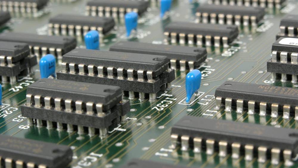
Mechanical methods have been widely used for years. They remain common due to lower upfront costs. However, they also have limitations.
V-cut depaneling uses pre-scored grooves on the PCB panel. A blade or linear separator applies force to break the board apart along the V-groove.
Advantages
· Fast process
· Lower equipment cost
· Suitable for simple board designs
Limitations
· Mechanical stress
· Limited design flexibility
· Risk of edge cracking
This method works best for rigid PCBs with straight cutting lines.
Routing Depaneling uses rotating cutting tools to separate boards. The machine physically mills around the PCB outline.
Advantages
· More flexible cutting paths
· Suitable for complex shapes
· Common in mass production
Limitations
· Tool wear
· Dust generation
· Burr formation
· Mechanical vibration
The routing process may affect delicate electronic components. Frequent maintenance is also required.
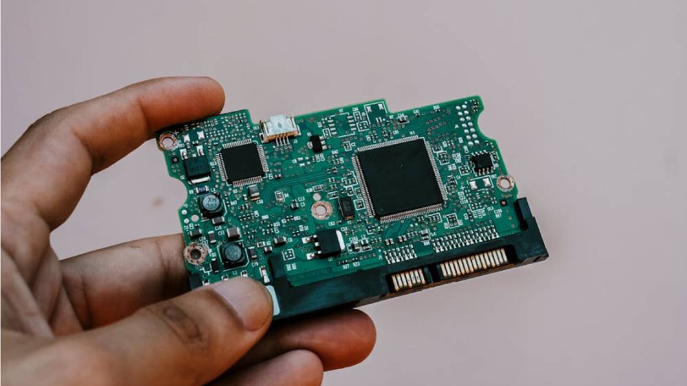
Punching uses molds or dies to separate boards through mechanical force. It is commonly used for high-volume production.
Advantages
· Fast cycle times
· Low cost per unit
Limitations
· High mechanical stress
· Limited flexibility
· Expensive tooling changes
Punching Depaneling is not ideal for thin or fragile circuit boards.
Traditional PCB depaneling methods share several challenges:
· Mechanical Stress: Physical force may damage solder joints and components. Stress-sensitive components are especially vulnerable.
· Burrs and Edge Damage: Mechanical cutting can leave rough edges. Extra post-processing may be required.
· Dust Contamination: Mechanical cutting creates debris. Dust can affect sensitive assemblies and reduce product reliability.
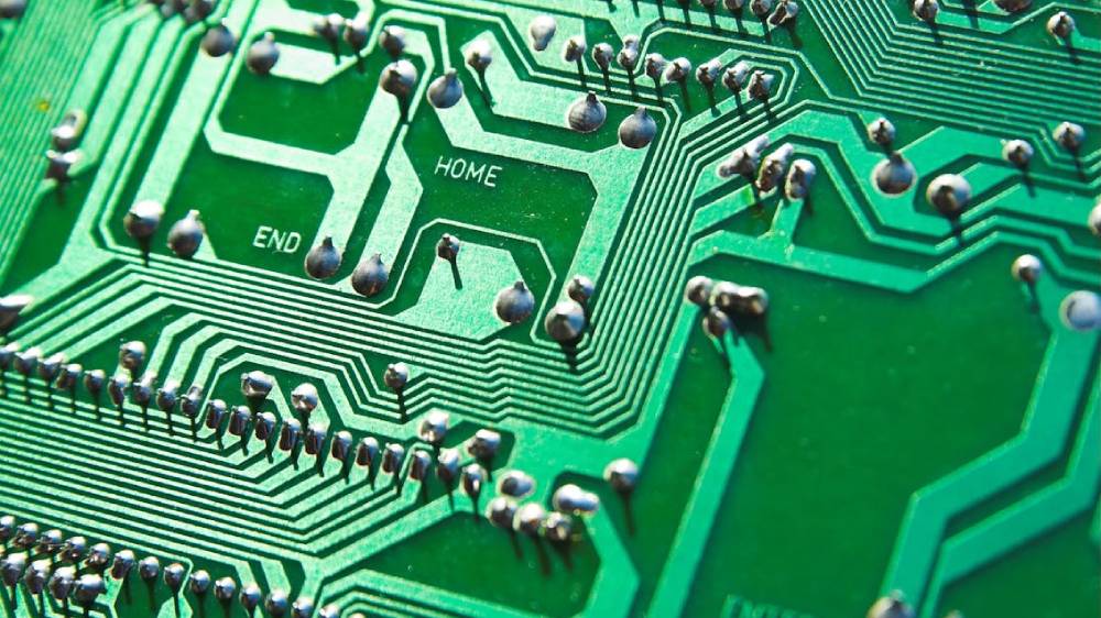
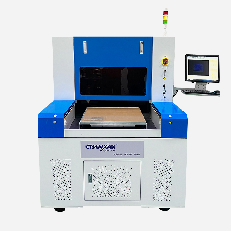
Laser depaneling uses focused laser energy to separate circuit boards without physical contact. Unlike routing or punching, there is no mechanical force applied to the PCB. This makes laser PCB depaneling ideal for high-precision electronics manufacturing.
Modern laser systems use nanosecond, picosecond, or femtosecond laser technology depending on the material and accuracy requirements. For information on the effects of different laser types, please refer to: Femtosecond vs Picosecond vs Nanosecond Lasers: Which Is Best for Precision Manufacturing?
High Precision: Laser systems can achieve micron-level cutting accuracy. This is essential for miniaturized electronics.
No Mechanical Stress: Because the process is non-contact, there is almost no stress transferred to the board. Sensitive components remain protected.
Clean Edges: Laser cutting reduces burr formation. Edge quality is significantly improved.
Better Automation: A modern PCB cutting machine with laser technology can integrate with automated production lines. This improves throughput and repeatability.
Flexible Design Capability: Complex shapes are easier to process. No tooling changes are required. This helps manufacturers shorten production lead times.
| Comparison Factor | Mechanical Depaneling | Laser Depaneling |
|---|---|---|
| Precision | Moderate | High micron-level precision |
| Mechanical Stress | High | Near-zero |
| Material Compatibility | Limited | Excellent for rigid, flex, and thin PCB |
| Maintenance | Tool replacement required | Lower maintenance |
| Automation | Moderate | High automation potential |
| Edge Quality | Burrs possible | Cleaner edges |
| Dust Generation | High | Minimal |
For advanced electronics, laser depaneling often provides better consistency and quality. Mechanical methods still work for low-cost, simple applications. However, complex electronics increasingly require non-contact PCB separation.
HDI PCB: HDI boards have narrow traces and compact layouts. Mechanical cutting may introduce stress damage. Laser depaneling offers higher precision and cleaner edges.
Rigid-Flex PCB: Rigid-flex designs are highly sensitive to stress. Traditional cutting methods may damage flexible sections. Laser-based PCB separation provides safer processing.
Thin PCB: Thin boards can easily crack during mechanical cutting. A laser PCB cutting machine minimizes force and improves yield.
The best method depends on your product and production requirements.
Choose mechanical methods if:
· Cost is the main concern
· Board designs are simple
· Stress sensitivity is low
Choose laser depaneling if:
· Precision matters
· Products use HDI or thin PCB
· Components are stress-sensitive
· Automation is important
· Product quality is critical
Manufacturers producing medical, automotive, or consumer electronics increasingly prefer laser-based solutions. The higher initial investment often leads to better long-term ROI. Lower defects. Less maintenance. Higher consistency.
Selecting the right PCB depaneling method directly impacts quality, yield, and manufacturing efficiency. Mechanical methods such as V-cut, routing, and punching remain useful for certain applications. However, they introduce stress, dust, and maintenance challenges.
For advanced electronics, laser depaneling offers clear advantages. Higher precision. Cleaner edges. Better automation. Minimal mechanical stress. As PCB designs continue to shrink, laser-based PCB separation is becoming the preferred solution for modern electronics manufacturing.
| Free solution
Previous: Top FPC Laser Cutting Equipment Manufacturers | How to Choose the Right Supplier
Next: FPC Laser Cutting Guide: Precision Solutions for Flexible PCB Manufacturing