Key Words: Silicon Wafer Dicing PCB Depaneling Glass Cutting
Home > News > Industry News
【Description】:
Discover how to choose the right wafer dicing laser solution for semiconductor manufacturing. This guide compares fiber, nanosecond, picosecond, and femtosecond laser systems for silicon, SiC, GaN, MEMS, and advanced packaging, helping manufacturers balance precision, speed, HAZ, and cost.
The semiconductor industry is rapidly evolving; the demand for smaller, thinner, and more powerful chips is pushing traditional manufacturing processes to their limits. With this, wafer dicing methods have shifted from mechanical sawing to advanced laser technologies. However, not all wafers are created equal. Different requirements—processing standard silicon or cutting-edge compound semiconductors like SiC and GaN—demand specific wafer dicing laser solutions. At Chanxan Laser, we provide a comprehensive range of wafer dicing equipment designed to meet the diverse needs of modern fabs, ranging from high-efficiency fiber lasers to ultra-precise picosecond and femtosecond platforms.
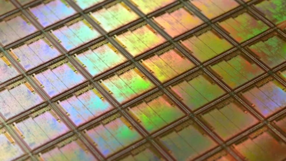
The choice of a laser wafer dicing machine depends on a complex interplay of material hardness, thermal sensitivity, and required kerf width. To simplify your decision-making process, we have categorized our solutions based on the industry's most common production scenarios:
| Wafer Dicing Requirement | Recommended Technology | Recommended Chanxan Machine | Best For |
|---|---|---|---|
| High-Speed Standard Dicing | High-Power Fiber Laser | CW-6060J | Silicon wafers, ceramic substrates, packaging materials, high-throughput production |
| High Precision & Controlled Thermal Impact | Nanosecond Laser | CW-6050Z | Precision wafer cutting, reduced HAZ processing, glass and ceramic substrates |
| Ultra-Fine Micro Dicing for MEMS & Optics | Picosecond Laser | CW-6050PZ | MEMS, optical chips, SiC/GaN wafers, fine-feature semiconductor processing |
| Semiconductor-Grade Cold Processing | Femtosecond Laser | CW-6050FZ | Ultra-thin wafers, advanced packaging, Micro LED, fragile semiconductor materials |
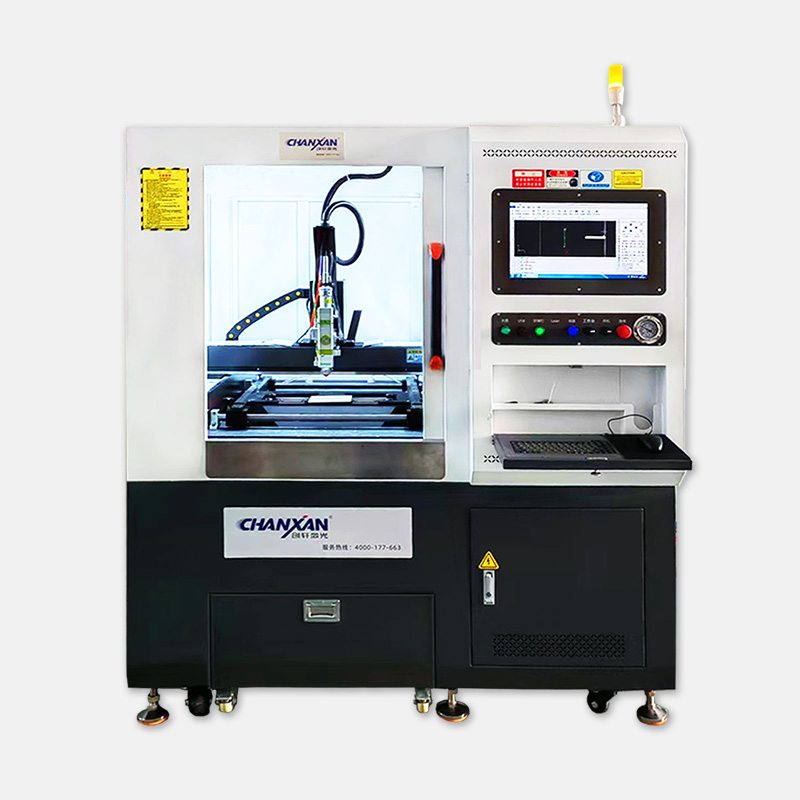
For manufacturers focused on throughput and cost efficiency on standard substrates, the CW-6060J High-Precision Fiber Laser Cutting Machine is the ideal workhorse. While advanced compound semiconductors require ultrafast pulses, standard silicon and ceramic packaging substrates benefit from the sheer power and stability of fiber laser technology.
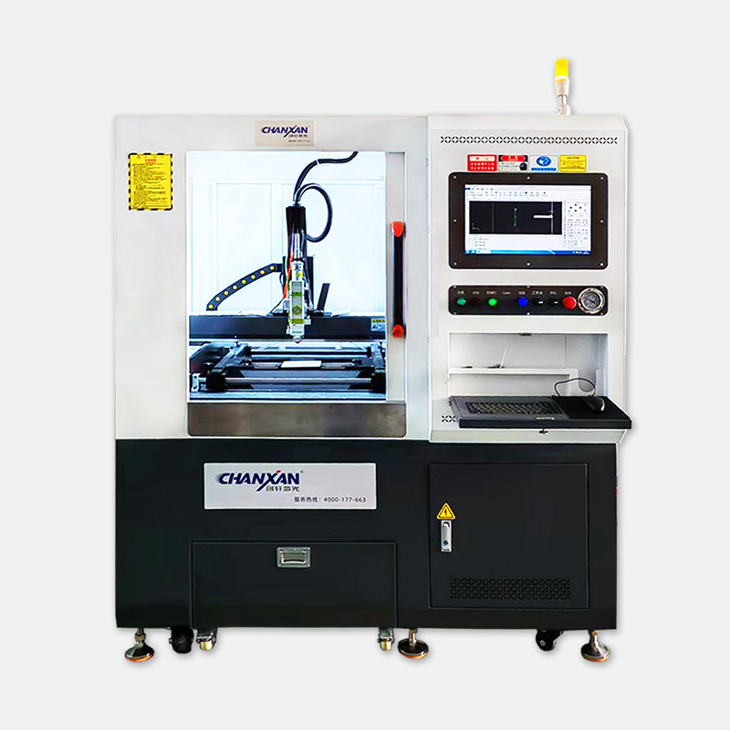
The CW-6060J is powered by a 1500W(Adjustable 5-95%) fiber laser (1070±5nm wavelength). Unlike low-power lasers, this high-wattage source allows for rapid penetration through thicker wafers and substrates.
•Precision Engineering: Equipped with an Akribis Linear Motor, the machine achieves a positioning accuracy of ±3 μm and a repetition accuracy of ±0.005 mm. In a high-volume production environment, this level of stability ensures that every "street" is cut with absolute consistency.
•Throughput Optimization: With a maximum speed of 60m/min and 1G acceleration, the CW-6060J is designed for speed. It significantly outpaces mechanical saws while eliminating the recurring costs of diamond blades.
•Thermal Management: To handle the 1500W power, we've integrated a dual-temp dual-control water cooling system (20-25℃), ensuring the laser source and optics remain at optimal temperatures during 24/7 operation.
Best Applications for Fiber Laser Dicing
The CW-6060J is the go-to wafer dicing equipment for:
•Silicon Wafer Dicing: Standard logic and memory chips where speed is the priority.
•Ceramic Substrates: Alumina or AlN substrates used in power modules.
•Packaging Substrates: Cutting through PCB-based or metalized substrates with high efficiency.
When to choose it: If your production line prioritizes speed and stable precision over ultra-low thermal impact, the CW-6060J offers the most cost-effective wafer dicing laser solution.
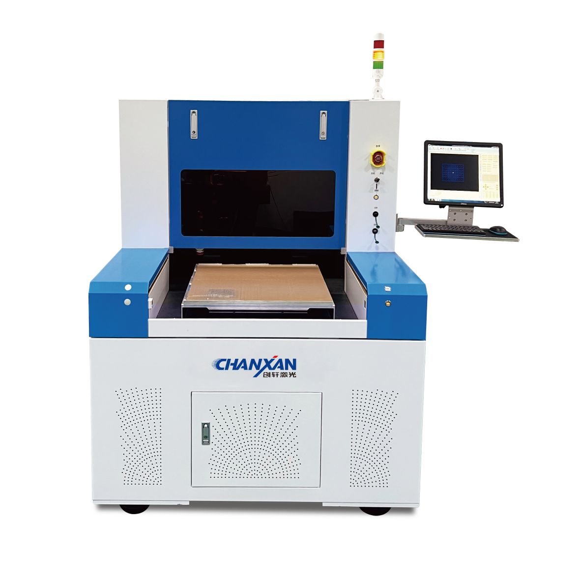
When your application involves thinner or more sensitive materials like glass or MEMS, the CW-6050Z Nanosecond Laser System offers a significant step up in quality. The nanosecond laser system delivers energy in short, controlled bursts (nanoseconds), significantly reducing the heat-affected zone (HAZ).
Key Technical Advantages:
•The CW-6050Z offers a versatile platform supporting UV, IR, or Green Nanosecond Lasers (15W). This allows manufacturers to select the wavelength that best matches their material's absorption profile.
•Controlled HAZ: By utilizing nanosecond pulses, the heat-affected zone is kept under ≤20μm. This prevents the warping or melting of delicate circuit features near the cut line.
•Micron-Level Positioning: The system boasts a ±1μm positioning and repeatability accuracy, making it suitable for high-density wafers where the streets are extremely narrow.
•Machining Accuracy: Overall accuracy of ≤25μm for intricate designs.
Ideal Use Cases
•Glass Wafers: Minimizing micro-cracking and chipping.
•Thin Ceramic Wafers: Providing clean edges for high-frequency components.
•MEMS Devices: Protecting sensitive moving parts from excessive thermal stress.
When to choose it: This wafer dicing equipment is perfect for buyers who need superior edge quality and lower thermal stress than fiber lasers while maintaining competitive productivity.
The rise of SiC (Silicon Carbide) and GaN (Gallium Nitride) has revolutionized the power electronics industry, but these materials are notoriously difficult to dice. They are extremely hard and brittle, making mechanical sawing slow and prone to high breakage rates. The CW-6050PZ Picosecond Laser System offers the ultimate solution through ultrafast laser wafer dicing.
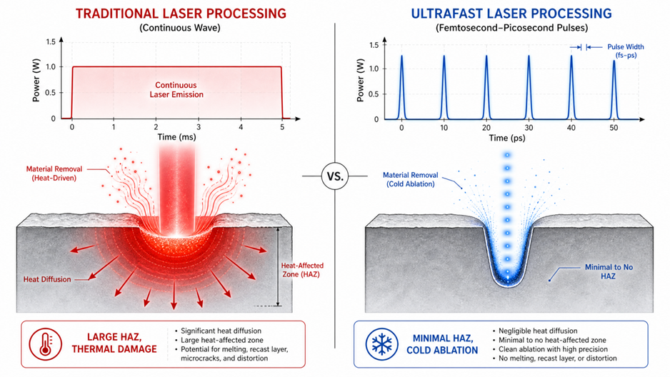
A picosecond is one-trillionth of a second. At this speed, the laser pulse delivers peak power so quickly that the material undergoes "cold ablation." The material is vaporized directly from solid to gas, bypassing the liquid phase.
•Minimal Micro-Cracks: Because there is virtually no melting, the structural integrity of the SiC or GaN wafer is preserved. This leads to significantly higher die strength and long-term reliability.
•Fine Pitch Capability: The CW-6050PZ can handle ultra-fine pitch requirements, allowing you to pack more dies onto a single expensive SiC wafer.
•High-Precision Platform: With a positioning accuracy of ±1μm and a customized adsorption platform (up to 1200mm*700mm), this machine is ready for the next generation of semiconductor packaging.
If you're looking for a wafer dicing solution that combines high precision and efficiency, the CW-6050PZ picosecond laser machine is designed for you. It reduces material waste and ensures that the electrical properties of high-bandgap semiconductors are not compromised by high temperatures.
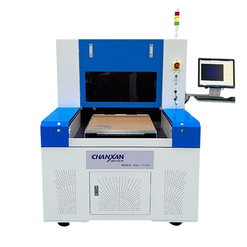
For the most demanding semiconductor-grade applications, the CW-6050FZ Femtosecond Laser System represents the pinnacle of wafer dicing laser solutions. Operating in the quadrillionths of a second, it achieves true cold processing, making it the only choice for ultra-thin or extremely fragile materials.
Key Technical Advantages:
•Zero Thermal Damage: The pulse duration is shorter than the time it takes for heat to transfer to the surrounding lattice. This results in an almost zero HAZ and a completely crack-free cut edge.
•Ultra-Thin Wafer Handling: As wafers are ground down to <100μm for advanced packaging, they become incredibly fragile. The non-contact, cold processing of the CW-6050FZ is the only way to ensure high yields for these ultra-thin chips.
•Precision Without Compromise: With ±1μm positioning and a machining thickness of ≤1mm, this system is ideal for Micro LED, optical chips, and advanced semiconductor fabs.
When to choose it: This is the premium solution for ultra-precision wafer dicing where yield is the absolute priority and material integrity cannot be compromised.
Although picosecond lasers currently hold a larger market share, the superior processing performance of femtosecond laser systems makes them ideal for future cutting-edge processes. For manufacturers with stringent requirements for precision and processing results, and who wish to maintain a leading edge in technology and performance, femtosecond laser machines are the best choice.
| Feature | Fiber LaserCW-6060J | Nanosecond LaserCW-6050Z | Picosecond LaserCW-6050PZ | Femtosecond LaserCW-6050FZ |
|---|---|---|---|---|
| Precision | Good (±3 μm) | Better (±1 μm) | High (±1 μm) | Highest (±1 μm) |
| Heat-Affected Zone (HAZ) | Moderate | Low (≤20 μm) | Very Low | Nearly Zero |
| Processing Type | Thermal Melting | Controlled Thermal Processing | Cold Ablation | Pure Cold Processing |
| Processing Speed | Fastest (60 m/min) | Fast (≤3000 mm/s) | Medium | Precision-Focused |
| Initial Investment | Lowest | Medium | High | Premium |
| Typical Applications | Standard silicon wafers, ceramics, packaging substrates | Glass wafers, MEMS, sensors, precision substrates | SiC, GaN, power semiconductors, optical chips | Ultra-thin wafers, Micro LED, fragile semiconductor materials |
Chanxan Laser has spent years engineering solutions specifically for the semiconductor industry. When you choose our wafer dicing laser machine, you are supported and backed by:
1. Semiconductor-Focused Engineering: Our machines are designed to meet the rigorous standards of modern cleanrooms and high-uptime production environments.
2. Ultrafast Laser Expertise: We specialize in integrating picosecond and femtosecond technology into stable, industrial-grade platforms.
3. Custom Automation & CCD Alignment: Every machine can be equipped with advanced CCD vision systems to ensure micron-level alignment on every wafer.
4. Global Support & Material Testing: We invite you to send us your materials for sample testing. Our engineers will provide a detailed process evaluation to ensure you get the right machine for your specific recipe.
Don't let outdated dicing methods bottleneck your yield. Contact Chanxan Laser today for a customized recommendation and discover how our wafer dicing laser solutions can transform your semiconductor manufacturing process.
| Free solution
Previous: Ultrafast Laser Technology: Principles, Comparison & Industrial Applications
Next: How to Choose a Wafer Dicing Machine: Buyer's Guide for Semiconductor Manufacturing