Key Words: Silicon Wafer Dicing PCB Depaneling Glass Cutting
Home > News > Industry News
【Description】:
Explore the complete guide to ultrafast laser technology — covering femtosecond laser systems, picosecond laser machines, nanosecond laser cutting machines, cold ablation principles, and real-world industrial applications across semiconductor, medical, and electronics manufacturing.
The global manufacturing industry is at an inflection point. As we move deeper into the Industry 4.0 era, the demand for higher precision, faster throughput, and zero thermal damage has made ultrafast laser technology one of the most transformative forces in modern production. The development of ultrafast lasers has met market demands and reduced operating costs. As a result, ultrafast laser equipment has evolved from laboratory research devices into industrial tools that facilitate production.
According to Fortune Business Insights, the global ultrafast laser market is projected to reach $10.26 billion by 2034, growing at a compound annual growth rate (CAGR) of 21.0% — significantly outpacing traditional laser technologies. This surge is driven by the explosive demands of the semiconductor, electric vehicle (EV) battery, and medical device sectors.
Based on the pulse characteristics of ultrafast lasers, this article provides an in-depth overview of three main ultrafast laser platforms—femtosecond laser systems, picosecond laser systems, and nanosecond laser systems—from both technical and application perspectives.
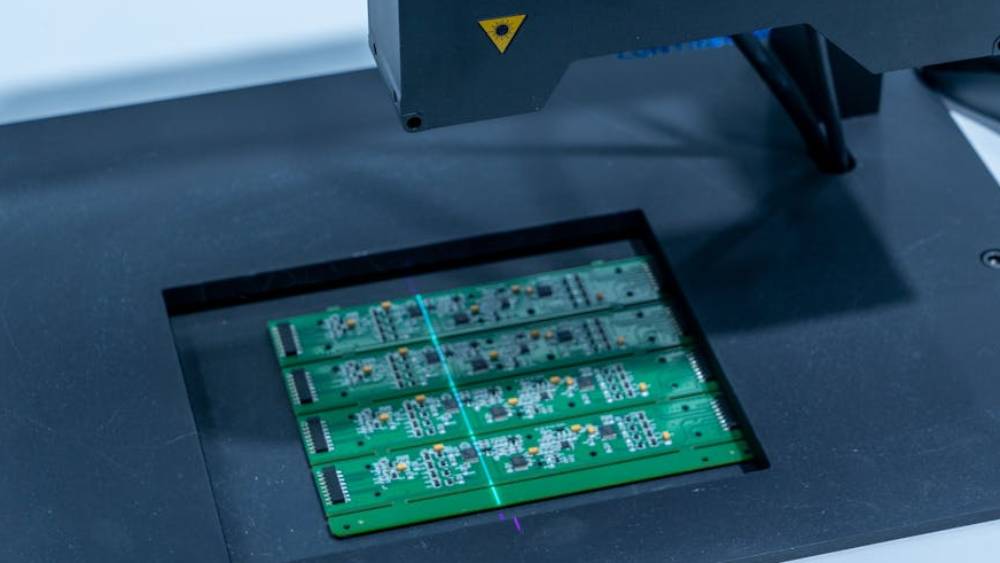
An ultrafast laser is defined by its ability to emit optical pulses with durations in the picosecond (10⁻¹² s) or femtosecond (10⁻¹⁵ s) range. The defining characteristic of any ultrafast laser system is the mechanism by which it removes material — not through melting or burning, but through a quantum-level process called cold ablation.
Traditional laser processing (including most nanosecond laser systems) relies on heat transfer: the laser heats the material until it melts or vaporizes. For delicate or heat-sensitive workpieces, this can leave heat-affected zones (HAZs), microcracks, recast layers, and debris during processing, which typically require secondary polishing or post-processing.
Ultrafast lasers — particularly femtosecond and picosecond platforms — operate on an entirely different physical principle. When an ultrashort pulse interacts with a material surface, the photon energy is instantaneously absorbed by free electrons. Because the pulse duration is shorter than the electron-to-lattice energy transfer time (the electron-phonon coupling time), the surrounding material lattice has no time to absorb thermal energy. The result is direct material ejection through multiphoton absorption and plasma formation — with virtually zero thermal diffusion into the surrounding area.
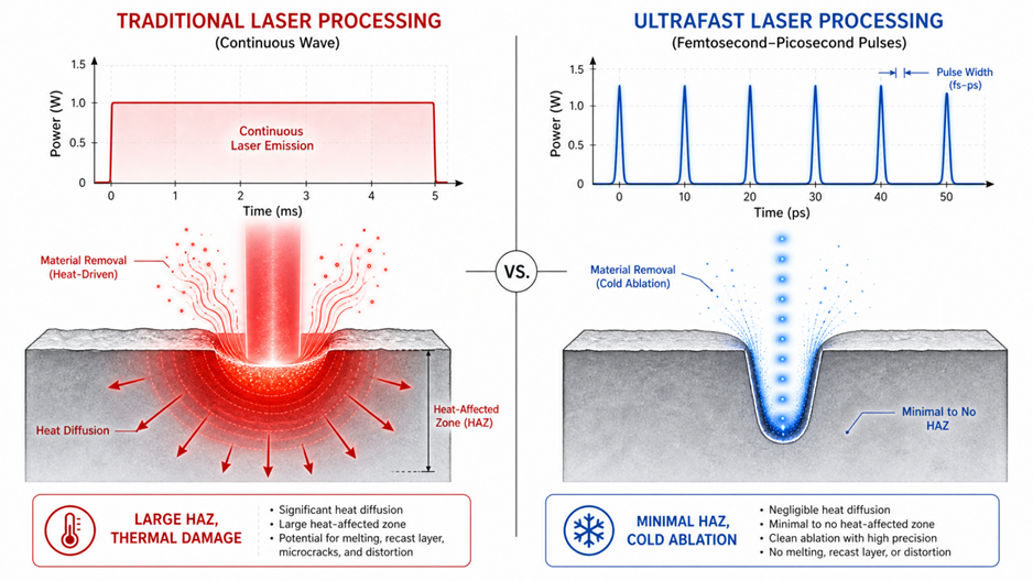
This is the essence of "cold processing": material is removed precisely and cleanly, preserving the original physical, chemical, and structural properties of the workpiece.
| Feature | Traditional Laser (Nanosecond) | Ultrafast Laser (Picosecond / Femtosecond) |
|---|---|---|
| Processing Mechanism | Thermal Melting & Vaporization | Cold Ablation |
| Heat-Affected Zone (HAZ) | Large — risk of melting and micro-cracking | Minimal to nearly zero |
| Edge Quality | Burrs, recast layer, micro-cracks may occur | Clean, sharp, polished edges |
| Post-Processing Requirement | Secondary polishing often required | Minimal to no post-processing |
| Suitability for Sensitive Materials | Limited — may damage polymers, thin films, and brittle materials | Ideal for glass, polymers, semiconductors, and bio-materials |
| Dimensional Precision | Typically ±10 μm or greater | Typically ±1–3 μm (sub-micron achievable) |
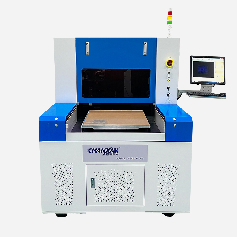
Manufacturers must select the right laser platform based on their material requirements, throughput demands, and precision targets. Chanxan Laser's three representative ultrafast laser platforms cover different needs at different levels of precision.
Specifications at a Glance:
Pulse Width: < 300 fs (femtoseconds)
Wavelength: 1030 nm (IR); also available in UV/Green harmonics
Positional Precision: ±1 μm
The femtosecond laser system represents the pinnacle of laser precision engineering. With pulse durations measured in units of 10⁻¹⁵ seconds, a femtosecond laser machine can achieve processing results that approach atomic-level accuracy. The near-perfect cold ablation mechanism makes this platform the definitive choice for applications where thermal damage is absolutely unacceptable.
A femtosecond laser cutting machine excels at processing ultra-thin and brittle materials — sapphire, ultra-thin glass (UTG), SiC wafers — where even nanoscale cracking would render a component unusable. In the medical device sector, femtosecond technology enables the fabrication of cardiovascular stents with wall thicknesses as low as 50 μm, with burr-free edges that meet the strictest biocompatibility standards.
Primary Industrial Applications of Femtosecond Laser Systems:
Semiconductor wafer dicing and TSV/TGV (Through-Silicon Via / Through-Glass Via) drilling
Advanced packaging processes in heterogeneous integration
Medical device micro-machining (heart stents, surgical instruments, ophthalmic tools)
Ultra-thin glass and sapphire cold cutting for foldable display manufacturing
Sub-micron micro-nano-fabrication for photonics and scientific research
Precision processing of heat-sensitive bio-tissues and polymer films
Best Suited For: Applications requiring the absolute highest precision, zero HAZ, and processing of heat-sensitive or ultra-brittle materials where no compromise on quality is acceptable.
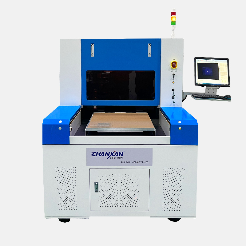
Specifications at a Glance:
Pulse Width: < 10 ps (picoseconds)
Wavelength: 532 nm (Green); also available in 1064 nm IR and UV harmonics
Positional Precision: ±3 μm
The picosecond laser system occupies the strategic sweet spot between femtosecond-level precision and industrial-scale throughput. A picosecond laser machine delivers pulse durations in the 10⁻¹² second range — still well within the ultrafast regime and achieving genuine cold ablation with minimal thermal impact, while offering significantly higher pulse repetition rates and processing speeds compared to femtosecond platforms.
For high-volume manufacturing environments, the picosecond laser cutting machine offers a compelling combination of excellent edge quality, high repeatability, and seamless integration with automated production lines. This makes it the workhorse platform for precision electronics manufacturing, where millions of identical components must be processed with consistent micron-level accuracy.
The picosecond laser is particularly effective on brittle materials such as glass and ceramics, where its controlled ablation profile prevents crack propagation. In consumer electronics, picosecond systems are widely deployed for OLED panel scribing, FPC (Flexible Printed Circuit) cutting, and UTG processing for next-generation foldable smartphones.
Primary Industrial Applications of Picosecond Laser Systems:
PCB (Printed Circuit Board) and FPC micro-drilling and cutting
OLED display panel scribing and edge finishing
Consumer electronics component processing (UTG, cover glass)
Brittle material removal — glass, alumina ceramics, borosilicate
High-volume precision industrial component manufacturing
Semiconductor back-end processing and wafer singulation
Best Suited For: High-volume industrial manufacturing environments where processing speed, repeatability, and automation compatibility are equally critical alongside precision.
Specifications at a Glance:
Pulse Width: < 20 ns (nanoseconds)
Wavelength: 1064 nm (IR)
Positional Precision: ±10 μm
The nanosecond laser system represents the mature backbone of industrial laser processing. While technically operating at the boundary of the ultrafast regime, a nanosecond laser machine delivers proven, cost-effective, and highly versatile solutions for a broad range of standard manufacturing tasks. Nanosecond pulses are long enough to generate controlled thermal interaction with the workpiece, making them highly effective for applications that benefit from — or require — thermal processing.
A nanosecond laser cutting machine excels in applications such as thick metal cutting, surface hardening, and deep engraving where material removal rates and throughput are the primary metrics. The nanosecond laser platform also remains the industry standard for high-speed marking and traceability applications across automotive, electronics, and industrial parts manufacturing.
As global manufacturing continues its transition toward finer feature sizes and tighter tolerances, many facilities are strategically deploying nanosecond laser systems for general manufacturing tasks while upgrading to picosecond or femtosecond platforms for their highest-precision operations.
Primary Industrial Applications of Nanosecond Laser Systems:
Industrial marking, engraving, and serialization (QR codes, DataMatrix, logos)
Metal welding and deep penetration joining
Surface treatment, annealing, and hardening
Thick material cutting and macro-scale ablation
General industrial manufacturing and component finishing
Best Suited For: Cost-sensitive, high-throughput industrial manufacturing where standard precision tolerances are acceptable and thermal processing is not a disqualifying factor.
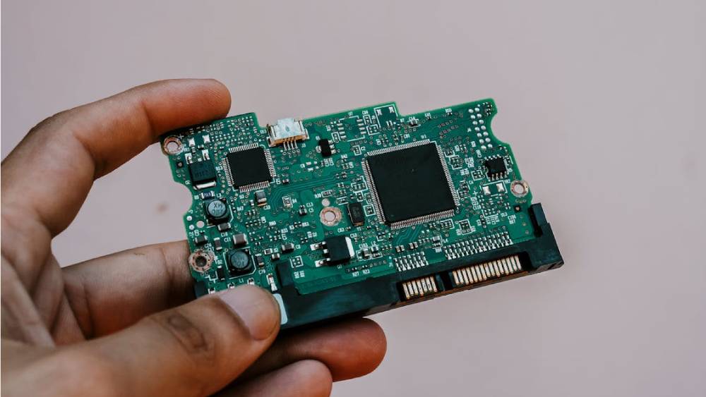
Femtosecond and picosecond platforms enable sub-micron wafer dicing, TSV drilling, and advanced packaging with zero chipping or delamination — critical for maintaining die yield in high-value compound semiconductor production (SiC, GaN, InP).
The femtosecond laser cutting machine and picosecond laser cutting machine are central to the manufacture of foldable smartphones, enabling perfect-edge UTG cutting and OLED panel scribing without the micro-fractures that destroy display longevity.
The strict biocompatibility and dimensional accuracy requirements of cardiovascular stents, minimally invasive surgical tools, and implantable devices make the femtosecond laser system the processing technology of choice. Burr-free, contamination-free edges are not optional — they are regulatory requirements.
Laser electrode cutting with ultrafast systems eliminates the metallic burrs and debris that can cause short-circuit failures in lithium-ion battery cells. The ultrafast laser machine has become a critical quality control technology in gigafactory production lines.
Surface texturing, waveguide writing, and optical microstructure fabrication demand the resolution only achievable with femtosecond laser systems — enabling next-generation AR/VR optics, LiDAR components, and photonic integrated circuits.
High-temperature alloys such as Inconel and titanium require the controlled, debris-free cutting of ultrafast laser systems to maintain the structural integrity of turbine blades, fuel injector nozzles, and thermal protection components.
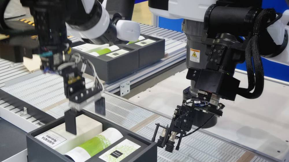
One of the most compelling attributes of modern ultrafast laser systems is their ability to process materials that defeat conventional laser or mechanical methods:
Hard & Brittle Materials: Silicon carbide (SiC), sapphire, alumina ceramics, quartz glass — materials that shatter under mechanical stress or crack under thermal loading are processed cleanly with cold ablation.
Highly Reflective Metals: Copper, gold, and aluminum — traditionally problematic for IR lasers due to high reflectivity — respond well to ultrashort pulses, enabling precise processing of EV battery busbars, RF connectors, and semiconductor leadframes.
Heat-Sensitive Substrates: Polymer films, flexible circuit substrates, bio-tissues, and thin-film coatings require the zero-HAZ processing that only femtosecond and picosecond platforms deliver.
Composite & Layered Structures: Carbon fiber reinforced polymers (CFRP), multi-layer laminates, and heterogeneous stacks are selectively ablated layer by layer with laser parameters tuned to each constituent material.
A fully engineered ultrafast laser system for industrial deployment integrates multiple precision subsystems:
Micro-Drilling: High-aspect-ratio holes with diameters in the micron range, enabling dense via arrays in PCBs, fuel injector spray holes, and MEMS structures — impossible to achieve with mechanical drilling at this scale.
Surface Texturing & Functionalization: Ultrafast laser surface texturing creates micro/nano structures that modify wettability, friction, optical reflectance, and cell adhesion — opening applications in biomedicine, optics, and tribology.
Thin Film Selective Ablation: Precisely removing one coating layer without disturbing the substrate — essential for thin-film solar cell scribing, OLED patterning, and flexible electronics manufacturing.
Complex Geometry Precision Cutting: 2D and 3D cutting of intricate geometries in ultra-thin materials, eliminating the tooling costs and geometric limitations of die-cutting or mechanical milling.

The convergence of several technology megatrends is accelerating ultrafast laser adoption beyond the early-adopter phase into mainstream industrial deployment:
Chiplet Architecture & Advanced Packaging: As Moore's Law slows, the semiconductor industry is moving toward chiplet integration and 3D stacking — processes that demand the sub-micron accuracy of femtosecond laser systems for inter-die interconnects.
Foldable & Rollable Display Manufacturing: Next-generation consumer devices require UTG cutting tolerances that are only achievable with picosecond and femtosecond laser cutting machines.
Solid-State Battery Production: The transition from liquid to solid-state electrolytes introduces new processing challenges — electrode cutting and electrolyte layer patterning — tailor-made for ultrafast laser machine solutions.
Photonic Integrated Circuits (PICs): The expansion of AI data center infrastructure is driving explosive demand for silicon photonics components, where femtosecond laser systems enable waveguide writing and fiber coupling structures at previously unachievable resolutions.
The decision between a femtosecond laser system, picosecond laser system, or nanosecond laser system is ultimately a strategic one — balancing precision requirements, production economics, and future application roadmaps.
For manufacturers operating at the frontier of precision — processing SiC wafers, foldable glass, cardiovascular implants, or photonic components — the femtosecond laser machine is not a premium option but an enabling technology. For the vast majority of precision electronics and industrial parts manufacturers, the picosecond laser cutting machine delivers an optimal balance of quality and throughput. And for established high-volume marking, welding, and general manufacturing operations, the nanosecond laser cutting machine remains a proven and cost-effective workhorse.
The common thread across all three platforms is clear: the future of precision manufacturing is ultrafast, cold, and clean. Whether your application demands a femtosecond laser cutting machine, a picosecond laser machine, or a versatile nanosecond laser system, partnering with a provider who offers deep application engineering expertise, a validated materials database, and robust automation integration capability is the key to unlocking the full potential of ultrafast laser technology.
A femtosecond laser operates with pulse durations below 1,000 femtoseconds (10⁻¹⁵ s), while a picosecond laser uses pulses in the range of 1–100 picoseconds (10⁻¹² s). Both are classified as ultrafast lasers and achieve cold ablation. Femtosecond systems offer superior precision and absolutely minimal HAZ; picosecond systems provide a better balance of precision and processing speed for high-volume production.
A nanosecond laser machine is the right choice when processing cost, throughput, and ease of operation are the primary factors, and when your application does not require sub-10 μm precision or involves thermally robust materials where some HAZ is acceptable. For applications involving heat-sensitive materials, brittle substrates, or micron-level tolerances, an ultrafast laser system is necessary.
Semiconductor manufacturing, advanced medical device fabrication (stents, surgical instruments), ophthalmic applications, photonics, and aerospace component manufacturing benefit most from femtosecond laser machines, where the combination of sub-micron precision and zero thermal damage is mission-critical.
Yes. The picosecond laser cutting machine is highly effective for glass, sapphire, and ceramic processing. The controlled cold ablation profile of picosecond pulses prevents crack propagation in brittle materials, enabling clean cuts and holes in cover glass, optical components, and display substrates.
Industrial femtosecond laser systems achieve ±1 μm positional accuracy; picosecond laser systems achieve ±3 μm; nanosecond laser systems typically achieve ±10 μm. These specifications are achievable with high-precision linear motion stages and active beam alignment systems integrated into the laser platform.
| Free solution
Previous: How to Choose the Right Ultrafast Laser: Picosecond vs Femtosecond vs Nanosecond
Next: Wafer Dicing Laser Solutions: Choosing the Right Machine for Semiconductor Precision