

Key Words: Silicon Wafer Dicing PCB Depaneling Glass Cutting
Home > News > Industry News
【Description】:
Learn how to choose the best wafer dicing machine for semiconductor manufacturing. Compare blade vs laser dicing, evaluate precision, automation, ultrafast laser technology, and discover why laser wafer dicing is becoming the preferred choice for Si, SiC, GaN.
The semiconductor industry is currently navigating a period of unprecedented transformation. As global demand for high-performance computing, electric vehicles (EVs), and IoT devices surges, the pressure on back-end-of-line (BEOL) processes has never been higher. Among these processes, wafer dicing—the act of singulating a finished wafer into individual chips—stands as a critical juncture where manufacturing efficiency meets product reliability. Choosing the right wafer dicing machine directly dictates your fab's yield, throughput, and bottom line.
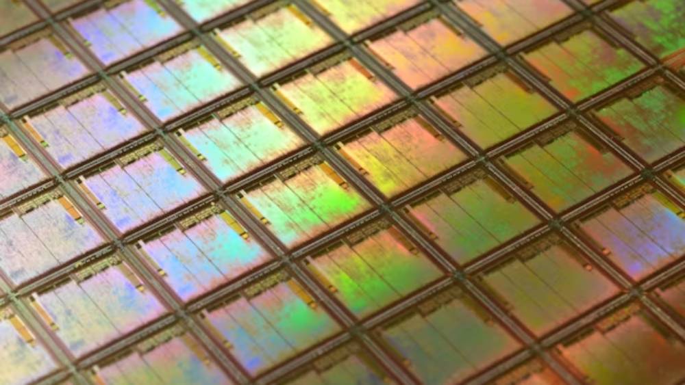
To make an informed choice, one must first understand the three dominant technologies shaping the market today. While mechanical sawing has been the industry workhorse for decades, the rise of fragile materials and ultra-thin wafers is rapidly shifting the preference toward laser-based solutions.
Feature | Mechanical Blade Dicing | Laser Dicing (Ablation/Stealth) | Plasma Dicing |
Mechanism | Physical diamond blade grinding | High-energy beam vaporization | Chemical reactive ion etching |
Best For | Standard Silicon, thicker wafers | Thin wafers, SiC, GaN, fragile substrates | Very small dies, high-density layouts |
Kerf Width | Wide (30–60 µm) | Narrow to Zero (0–20 µm) | Extremely Narrow (<5 µm) |
Mechanical Stress | High (risk of chipping/cracking) | Zero (non-contact) | Zero |
Capital Cost | Moderate | High | Very High |
Mechanical Blade Dicing remains cost-effective for standard logic chips on thicker silicon substrates. However, it introduces significant mechanical stress, leading to backside chipping and potential die-body cracks. In contrast, Laser Wafer Dicing has emerged as the modern standard. It offers non-contact processing, which is essential for the fragile compound semiconductors like Silicon Carbide (SiC) and Gallium Nitride (GaN) that power modern power electronics.
When evaluating potential equipment manufacturers, buyers must look beyond the price tag and focus on five core technical pillars:
The first question any buyer should ask is: "What materials will I be processing tomorrow?" While silicon is ubiquitous, the industry is moving toward "Wide Bandgap" materials. A machine that excels at silicon might struggle with the hardness of sapphire or the brittleness of GaN. High-end laser systems, particularly those utilizing ultrafast laser (picosecond or femtosecond) pulses, provide the versatility to handle multiple substrates with a single platform by simply adjusting the laser parameters.
The drive toward thinner devices (smartphones, wearables) means wafers are often ground down to less than 100 µm before dicing. Mechanical blades often struggle with these "paper-thin" wafers, causing high breakage rates. Stealth Dicing, a subset of laser technology that focuses the beam inside the wafer to create a "stealth" layer before expansion, is the gold standard for thin-wafer singulation as it produces zero kerf and maximizes the number of dies per wafer.
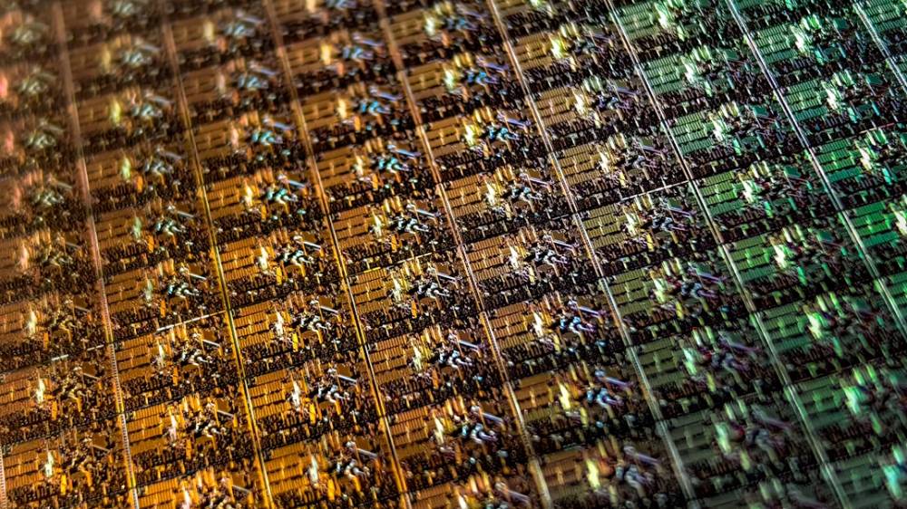
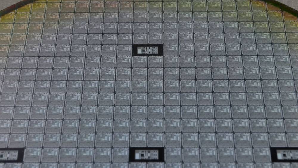
In semiconductor manufacturing, "streets" are the spaces between dies where the cut is made. The wider the street, the fewer chips you get per wafer. By choosing a machine with higher precision and a narrower kerf (cut width), manufacturers can reduce street dimensions, effectively increasing the "Gross Dies Per Wafer" (GDPW). This optimization often pays for the machine's cost through increased yield within the first year of operation.
In 2026, manual handling is a liability. Modern dicing machines must feature CCD Vision Alignment for micron-level accuracy and automated loading/unloading systems. For high-volume environments, look for dual-spindle designs (in blade saws) or high-repetition-rate lasers that can maintain high feed speeds without compromising cut quality.
The transition from mechanical to laser dicing is driven by the physics of miniaturization. As chips get smaller, the ratio of the "Heat Affected Zone" (HAZ) to the die size becomes more critical. Traditional lasers could cause thermal damage, but modern ultrafast lasers perform "cold" ablation. This means the material is vaporized so quickly that heat doesn't have time to transfer to the surrounding circuit, ensuring the electrical integrity of the die remains pristine.
Furthermore, the "Toolless" nature of laser dicing eliminates the recurring cost of diamond blades and the downtime associated with blade changes. This makes laser systems increasingly competitive on a Total Cost of Ownership (TCO) basis over a 3-to-5-year horizon.
Among the global players, Chanxan Laser has carved out a reputation for delivering semiconductor-grade precision through advanced laser engineering. Their approach addresses the most common pain points faced by modern fabs:
• Ultrafast Laser Integration: By utilizing picosecond and femtosecond laser sources, Chanxan systems achieve virtually zero carbonization and minimal HAZ, making them ideal for sensitive MEMS and power devices.
• Micron-Level Motion Control: Their equipment features high-resolution linear motors and advanced CCD alignment algorithms that ensure every cut is perfectly centered in the street, even on distorted or warped wafers.
• Tailored Automation Solutions: Chanxan Laser offers a range of wafer dicing equipment, from fiber laser wafer dicing systems to advanced ultrafast laser wafer dicing systems that meet even higher precision requirements, catering to diverse user needs for precision and cutting. Furthermore, they provide integrated workflows, including vision recognition systems, multiple selectable light source configurations, and computer-controlled flexible cutting shapes.
• Global Technical Support: Recognizing that downtime is catastrophic in semiconductor manufacturing, Chanxan provides robust overseas support and process validation services, allowing buyers to test their specific materials before making a final commitment.
To simplify your procurement process, consider the following scenarios:
• Scenario A: High-Volume Standard Silicon. If you are processing 300mm silicon wafers for low-cost logic chips, a high-speed, dual-spindle mechanical saw may still offer the best ROI.
• Scenario B: Fragile or High-Value Compound Semiconductors. For SiC, GaN, or thin-wafer applications, an Ultrafast Laser Dicing Machine (like those from Chanxan) is mandatory to prevent yield loss.
• Scenario C: R&D and Prototyping. Look for a versatile, small-footprint laser system that allows for rapid parameter changes across different materials without the need for custom tooling.
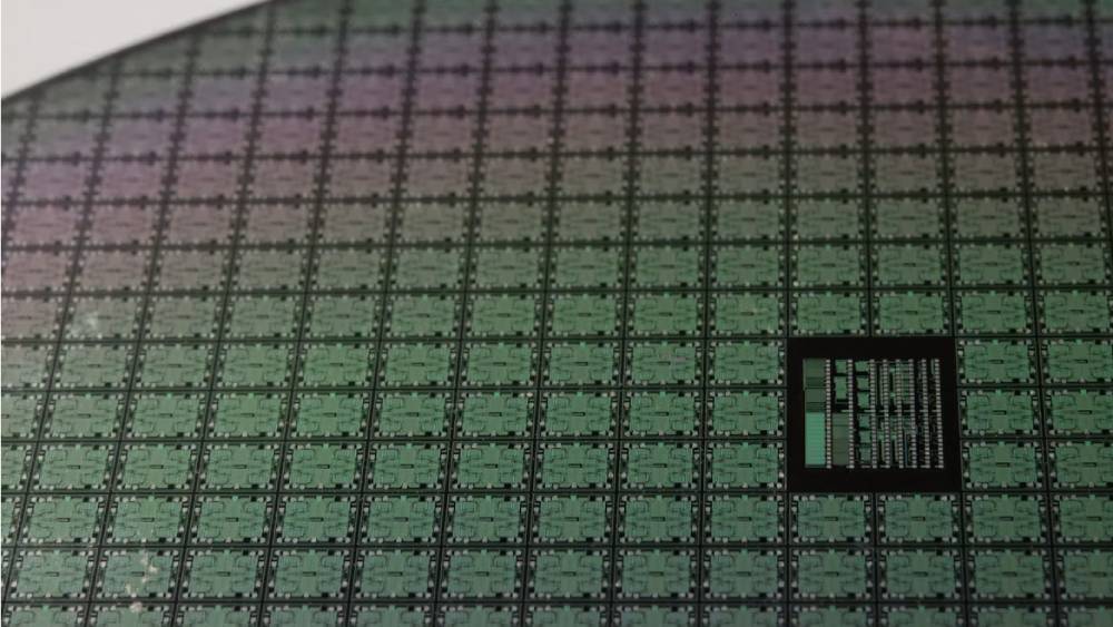
Choosing a wafer dicing machine requires a balance between current production needs and future technological shifts. As the industry moves toward smaller, thinner, and more complex devices, the limitations of mechanical dicing become more apparent. Investing in advanced laser technology is no longer a luxury—it is a prerequisite for survival in the high-yield semiconductor landscape.
When making your final selection, prioritize manufacturers that offer process validation and ultrafast laser expertise. Partners like Chanxan Laser provide the technical bridge between today's requirements and tomorrow's innovations, ensuring your fab remains at the cutting edge of semiconductor manufacturing.
| Free solution
Previous: Wafer Dicing Laser Solutions: Choosing the Right Machine for Semiconductor Precision
Next: Top FPC Laser Cutting Equipment Manufacturers | How to Choose the Right Supplier








