Key Words: Silicon Wafer Dicing PCB Depaneling Glass Cutting
Home > News > Industry News
【Description】:
Explore why 532nm green laser technology is the preferred choice for cutting copper substrates in power electronics. Learn about absorption mechanics and Chanxan Laser solutions.
TL;DR (Too Long; Didn't Read)
In power electronics manufacturing, copper substrates are essential for handling high currents and managing thermal dissipation. However, copper is notoriously difficult to process with standard industrial lasers due to its extreme thermal conductivity and high optical reflectivity. Green laser technology (532nm) has emerged as the premier choice for copper cutting because its wavelength achieves a dramatically higher material absorption rate compared to traditional infrared (IR) lasers. This enables stable, high-precision processing at lower peak power thresholds, completely eliminating the risk of catastrophic back-reflection damage to optical components while ensuring dross-free, highly conductive cut edges.
Standard industrial lasers, such as fiber or Nd:YAG systems, operate in the near-infrared (IR) spectrum (around 1064nm). At this wavelength, solid copper acts as a near-perfect mirror, reflecting the vast majority of the laser energy away from its surface. To force an IR laser to cut copper, operators must apply immense peak energy to melt the material. This creates an inherently unstable process: the moment the copper liquefies, its absorption increases abruptly, leading to uncontrollable micro-explosions, heavy slag formation, and back-reflections that can travels back up the optical path, destroying expensive laser engines.
Green laser technology solves this bottleneck at the atomic level. By passing a fundamental infrared beam through a non-linear frequency-doubling crystal, the wavelength is halved to 532nm. At this green spectrum, copper's material absorption increases significantly compared to infrared. Because the copper absorbs the green light efficiently right from the start of the pulse, the melting process begins smoothly and predictably, bypassing the volatile threshold phase entirely.
Copper is one of the best thermal conductors available, meaning it rapidly siphons heat away from the laser's impact zone into the rest of the panel. Green lasers concentrate energy so efficiently into the substrate that material vaporization happens faster than the copper can conduct the heat away. This drastically shrinks the localized Heat Affected Zone (HAZ), preventing the thin, high-density trace delamination, structural warping, and oxidation that frequently compromise power electronic modules.
The following comparison details the structural and quality differences when cutting industrial-grade pure electronic copper sheets:
| Processing Dynamics | Standard Near-Infrared Laser (1064nm) | Green Laser Technology (532nm) |
|---|---|---|
| Initial Material Absorption | Extremely Low (Highly reflective) | Significantly Higher (Efficient coupling) |
| Process Stability & Consistency | Volatile (Prone to sudden energy spikes) | Stable (Controlled, smooth energy deposition) |
| Optical Back-Reflection Risk | Severe (High risk of internal component damage) | Negligible (Safe for prolonged production) |
| Edge Dross and Slag Accumulation | Heavy (Requires aggressive post-machining deburring) | Minimal to Zero (Clean, burr-free cross-section) |
| Heat Affected Zone (HAZ) Profile | Wide (Risk of localized material warping) | Ultra-Narrow (Preserves material conductivity) |
Q: Why not use blue lasers (approx. 450nm) instead of green lasers for copper?
A: While blue lasers offer high absorption on copper, they are typically limited to continuous-wave (CW) direct diode configurations, which yield a relatively large focused spot size. Green lasers, however, can be configured as Q-switched short-pulse or ultrafast picosecond engines. This allows power electronics manufacturers to combine excellent absorption with high peak power density and microscopic focal spots, making green lasers superior for precision profiling and micro-vias.
Q: Does green laser cutting alter the electrical conductivity of the copper edge?
A: No. Because green laser processing minimizes thermal diffusion into the sidewalls, it avoids severe oxidation layers. The cut edge retains its pristine chemical composition and native electrical characteristics, which is critical for downstream heavy-wire bonding and soldering processes in power modules.
Q: What is the maximum thickness of copper that green lasers can cleanly process?
A: Green lasers excel at high-precision foil cutting and profiling thin-to-medium copper substrates commonly used in direct bonded copper (DBC) and insulated metal substrates (IMS). For ultra-thick busbars, a multi-pass scanning strategy can be deployed to maintain straight sidewalls without widening the kerf line.
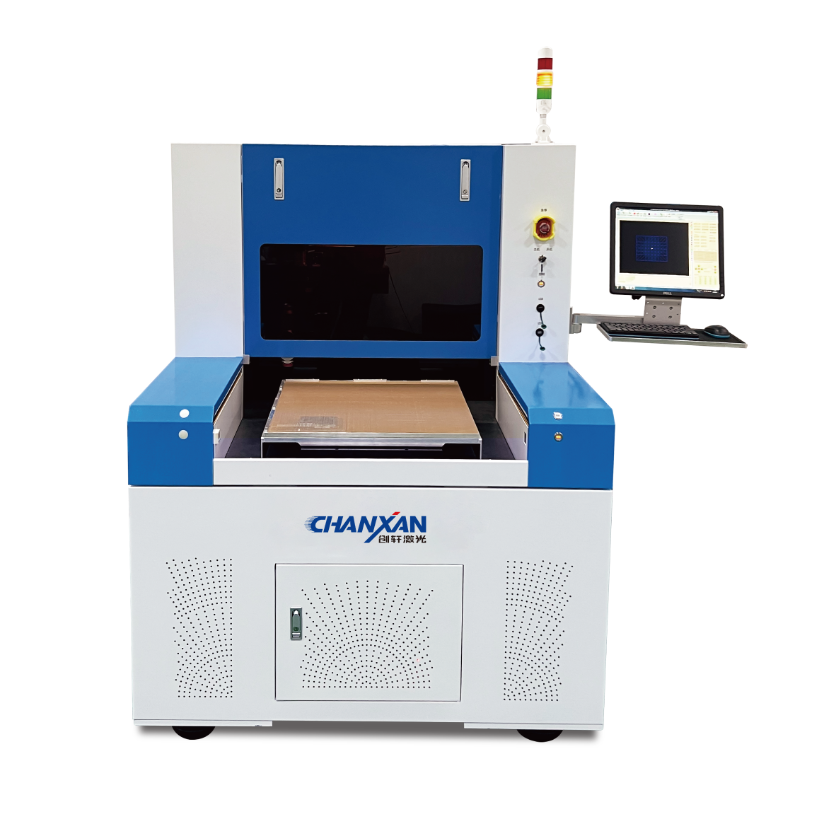
To meet the strict quality standards of the power electronics and semiconductor sectors, Chanxan Laser has engineered a specialized fleet of workstations optimized for highly reflective materials:
Chanxan Ultrafast Picosecond Green Laser Workstation: Combining high absorption with ultra-short pulse widths, this system achieves true "cold ablation" for ultra-dense power packaging, ensuring micrometric accuracy, vertical sidewalls, and a near-zero heat-affected zone without micro-cracking or burrs.
Disclaimer: To protect intellectual property and honor customer Non-Disclosure Agreements (NDAs), specific corporate background details in this industry scenario have been anonymized. However, all technical processing parameters, workflow data matrices, and operational cost-effectiveness metrics remain fully verified by Chanxan Laser's engineering applications laboratory.
| Free solution
Previous: CO2 vs. UV Laser for Ceramic Substrate Dicing: How to Choose?
Next: How Do You Avoid Micro-Cracks When Drilling Alumina Ceramics with Lasers?