

Key Words: Silicon Wafer Dicing PCB Depaneling Glass Cutting
Home > News > Industry News
【Description】:
Learn how semiconductor wafer dicing works, compare blade, laser, stealth, and plasma dicing methods, and explore the best solutions for silicon, SiC, GaN, and sapphire wafer cutting. Discover why laser wafer dicing is becoming a key technology in advanced semiconductor manufacturing.
Before discussing wafer cutting, it's essential to first distinguish between two different semiconductor processes: wafer slicing and wafer dicing. Although both involve cutting, they occur at different stages of semiconductor manufacturing.
Wafer slicing happens earlier in production. Large semiconductor crystal ingots are cut into thin wafers using diamond wire saws, also known as wire saw cutting or multi-wire sawing. This process creates the wafer substrates used in chip manufacturing and is widely applied for silicon, SiC, sapphire, and other semiconductor materials. Today, diamond wire sawing remains the mainstream method for wafer production because it enables relatively efficient and uniform slicing of hard materials.
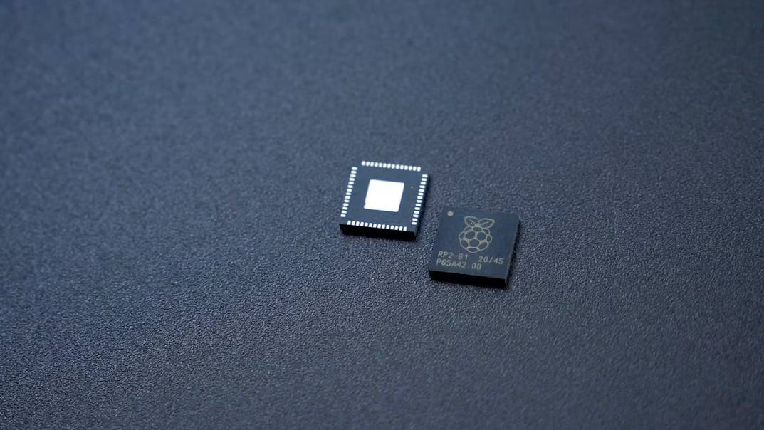
By comparison, wafer dicing takes place much later in semiconductor manufacturing. After photolithography, etching, deposition, and testing are completed, a processed wafer still contains hundreds or even thousands of semiconductor devices. At this stage, the wafer must be separated into individual chips, also known as dies, through a process called wafer dicing or die singulation. This step directly affects chip quality, yield, and reliability. Even microscopic defects introduced during cutting may reduce die strength or increase long-term failure risk.
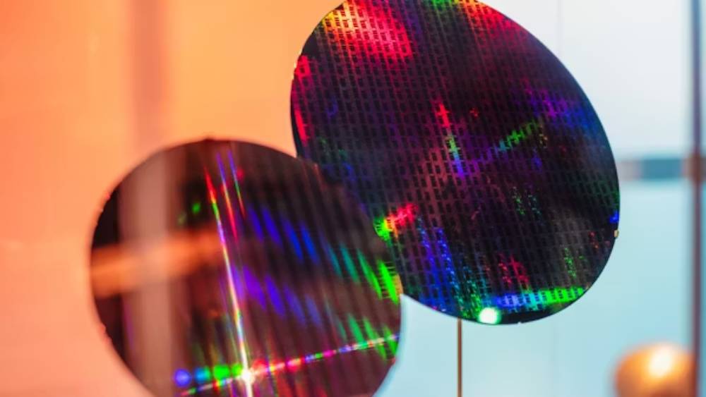
This guide focuses on semiconductor wafer dicing—how it works, the major technologies used today, and how manufacturers choose the right wafer cutting method for different materials and applications.
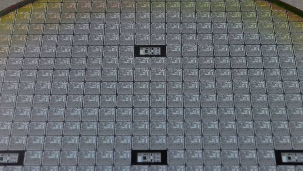
After wafer fabrication is completed, a semiconductor wafer contains hundreds or even thousands of individual chips arranged in a highly organized layout. These chips are separated by narrow spaces called dicing streets or scribe lines, which are intentionally designed to allow later singulation.
At this stage, the wafer has already gone through highly complex manufacturing steps such as photolithography, deposition, etching, and electrical testing. However, the chips still remain connected on a single wafer.
The purpose of wafer dicing is to precisely separate these chips into individual dies without damaging delicate device structures. Depending on the dicing technology used, manufacturers may cut through the wafer using a rotating blade, create controlled break lines, remove material with laser energy, or modify internal wafer layers for separation.
During this process, manufacturers must carefully control several critical factors:
Cutting precision
Kerf width
Chipping risk
Thermal damage
Mechanical stress
Particle contamination
Even very small defects created during wafer cutting may affect chip yield, packaging reliability, or long-term device performance.
There is no single solution for wafer dicing. Manufacturers choose different wafer cutting methods depending on:
Wafer material
Wafer thickness
Chip density
Yield requirements
Production goals
Today, mainstream semiconductor wafer cutting technologies can be divided into three major categories: mechanical dicing, laser wafer dicing, and plasma dicing.
Mechanical dicing remains widely used in semiconductor manufacturing, especially for standard silicon wafers and cost-sensitive production.
Blade dicing is the most established wafer cutting technology. This method uses a high-speed rotating diamond blade to physically cut through the wafer along predefined dicing streets.
Because of its mature process, stable throughput, and relatively lower operating cost, blade dicing is still widely adopted for high-volume semiconductor production. However, because the blade directly contacts the wafer, the process may introduce:
Edge chipping
Micro-cracks
Particle contamination
Mechanical stress
Blade wear
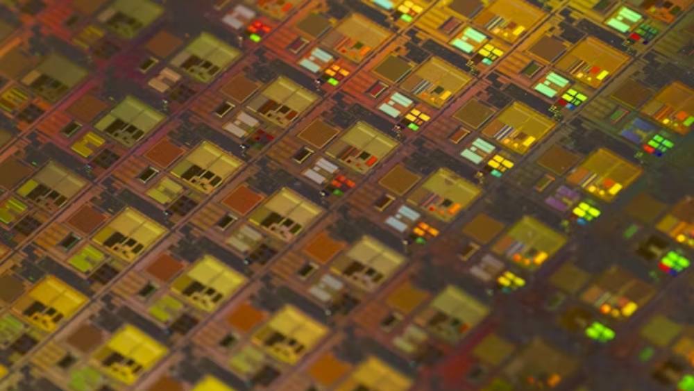
Scribe and break is another traditional singulation method. Instead of fully cutting through the wafer, shallow scribe lines are first created. Mechanical force is then applied to separate the wafer along these lines.
The method is relatively simple and economical. However, compared with modern dicing technologies, it provides lower precision and limited compatibility with advanced semiconductor structures. For fragile materials and complex chip layouts, yield limitations may become more noticeable.
As semiconductor manufacturing continues to evolve, laser wafer dicing is becoming increasingly used. Unlike mechanical cutting, laser systems process wafers without physical contact, helping reduce mechanical stress and eliminate blade wear.
Today, the two most common laser wafer dicing methods are:
Laser ablation dicing
Stealth dicing
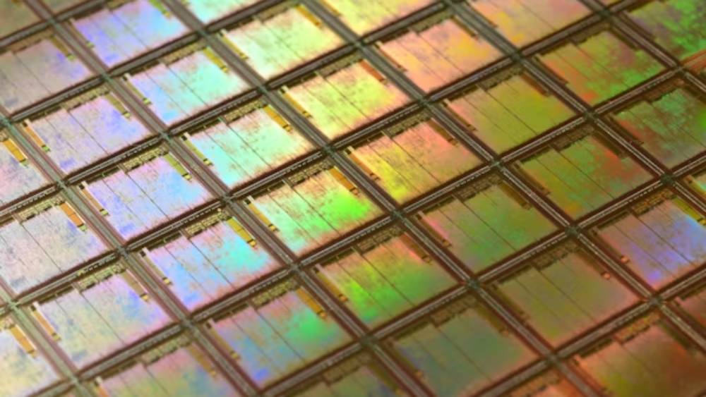
Laser ablation dicing works by using laser energy to remove material along the cutting path directly. This method is considered a surface-cutting process because material is removed from the wafer surface to create separation.
Compared with blade dicing, laser ablation provides several advantages:
Non-contact processing
Higher precision
Better flexibility for fine structures
Lower mechanical stress
Modern semiconductor wafer cutting machines increasingly adopt ultrafast picosecond or femtosecond lasers to reduce thermal damage and improve cutting quality.
Stealth dicing is also a form of laser wafer dicing, but its working principle is very different. Instead of cutting from the surface, the laser focuses energy inside the wafer, creating an internal modified layer beneath the surface. The wafer is later separated through controlled expansion and stress release.
Because material is not directly removed from the surface, stealth dicing offers several important advantages:
Minimal debris generation
Reduced chipping risk
No blade wear
Extremely low kerf loss
Better die strength
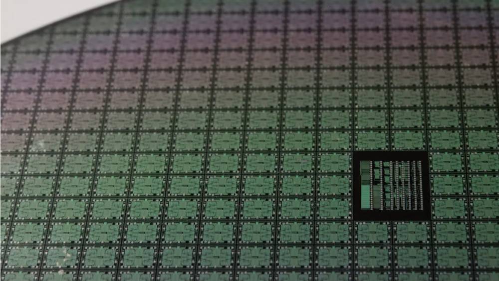
Plasma dicing belongs to another category of advanced non-mechanical wafer singulation. Unlike laser dicing, plasma dicing does not use laser energy. Instead, it relies on dry plasma etching to separate semiconductor dies.
Because no mechanical contact occurs, plasma dicing can achieve:
Extremely narrow dicing streets
Low mechanical stress
High precision for advanced semiconductor structures
However, plasma dicing generally involves more complex process integration and higher equipment cost, which limits adoption mainly to advanced semiconductor manufacturing environments.
Different wafer dicing methods offer different trade-offs in precision, cost, yield, and material compatibility. The table below compares the most widely used semiconductor wafer cutting technologies:
| Method Category | Dicing Method | Contact Type | Precision | Material Damage | Tool Wear | Suitable Materials | Main Advantages | Main Limitations |
|---|---|---|---|---|---|---|---|---|
| Mechanical | Blade Dicing | Contact | High | Medium–High | High | Silicon wafers | Mature, productive, lower cost | Chipping, debris, kerf loss |
| Mechanical | Scribe & Break | Partial Contact | Medium | Medium–High | Low | Standard brittle wafers | Simple and economical | Lower precision |
| Laser | Laser Ablation Dicing | Non-contact | High | Low | None | Silicon, thin wafers | Flexible, precise, lower stress | Potential thermal effects |
| Laser | Stealth Dicing | Non-contact | Very High | Very Low | None | SiC, GaN, ultra-thin wafers | Minimal damage, low kerf loss | Higher equipment cost |
| Advanced Non-Mechanical | Plasma Dicing | Non-contact | Very High | Very Low | None | Thin wafers, fine-pitch devices | Narrow streets, low stress | Process complexity, high cost |
The growing interest in laser wafer dicing is closely linked to changes in semiconductor manufacturing. Traditional cutting methods were developed for thicker silicon wafers and larger device structures. Today, semiconductor manufacturers increasingly work with:
Thin wafers
Narrow streets
High-value dies
Brittle materials
Complex package structures
These changes increase the demand for lower-damage cutting solutions.
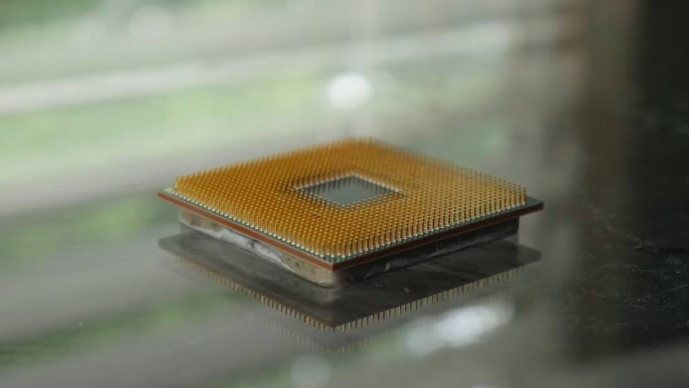
Laser ablation works by directly removing material from the wafer surface. Modern systems increasingly use ultrafast lasers, which generate extremely short pulses.
Ultrafast laser processing, particularly with femtosecond and picosecond pulses, achieves what is known as "cold ablation". This phenomenon is attributed to the extremely short pulse duration, typically in the range of femtoseconds (10⁻¹⁵ s) to picoseconds (10⁻¹² s). When these ultrashort pulses interact with a material, the photon energy is absorbed by electrons, leading to rapid electron excitation. The energy transfer from electrons to the lattice (phonons) occurs on a timescale longer than the pulse duration. Consequently, the material is removed through processes like multiphoton absorption and plasma formation before significant thermal diffusion can occur into the surrounding material. This minimizes the heat-affected zone (HAZ) and prevents thermal damage—a critical advantage over conventional laser processing.
For manufacturers, this means:
Cleaner edges
Lower chipping risk
Better precision
Improved product consistency
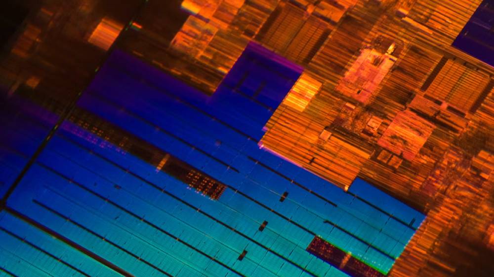
Different semiconductor materials require different wafer cutting strategies. Let's explore the most important material systems:
Traditional silicon wafer cutting remains widely used for CPUs, sensors, logic chips, and memory devices. Depending on chip design and yield requirements, manufacturers may choose blade dicing or laser dicing.
SiC wafer dicing is becoming increasingly important due to EV growth. SiC semiconductors support higher voltage, better thermal performance, and higher efficiency in electric vehicle power systems. However, SiC is harder and more brittle than silicon. Conventional blade cutting may increase cracking risk, making laser wafer dicing increasingly attractive.
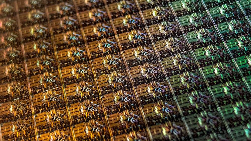
GaN devices are widely used in fast chargers, RF systems, and high-frequency electronics. Because these devices often require precise cutting and delicate structures, laser processing is increasingly adopted.
Sapphire wafers are commonly used in LED manufacturing and optical devices. Due to material hardness and brittleness, precision laser wafer cutting often provides better edge quality.
Choosing the right wafer dicing method depends on manufacturing priorities. The first consideration is material type. For standard silicon production, blade dicing may still be economical. However, harder materials such as SiC, GaN, or sapphire often require more advanced cutting methods.
The second factor is wafer thickness. Ultra-thin wafers are highly sensitive to mechanical force. In these cases, laser wafer dicing may help reduce stress and improve yield.
Manufacturers should also evaluate:
Edge quality requirements
Chip density
Yield targets
Production speed
Cost efficiency
Device sensitivity
For high-volume standard production, blade dicing may remain practical. But for advanced semiconductor manufacturing, where precision and material quality matter most, many manufacturers are increasingly evaluating semiconductor wafer cutting machines based on ultrafast laser technology.
Wafer dicing directly impacts chip quality, yield, and overall manufacturing efficiency. For silicon, SiC, GaN, and sapphire wafers, manufacturers need a balanced solution—one that offers high precision, minimal material damage, and adaptability to different wafer types.
Laser wafer dicing provides this balance. Its non-contact processing, reduced mechanical stress, low kerf loss, and compatibility with advanced materials make it ideal for modern semiconductor production.
To fully leverage these advantages, integrated systems are key. Chanxan's ultrafast laser dicing solutions combine high-speed processing with precision control, enabling manufacturers to singulate wafers efficiently while maintaining die quality across a variety of materials.
This integrated approach ensures optimal performance, higher yield, and better reliability, making it a strategic choice for next-generation semiconductor manufacturing.
Get Your Customized Solution| Free solution
Previous: FPC Laser Cutting Guide: Precision Solutions for Flexible PCB Manufacturing
Next: How Semiconductor, PCB, and FPC Work Together in Electronics








