1. Introduction: The Role of Laser Scribing in Photovoltaic Manufacturing
In the production of thin‑film photovoltaic (PV) devices, laser scribing is an essential process that directly determines the electrical performance and yield of solar panels. Thin‑film solar cells—such as those based on amorphous silicon (a‑Si), cadmium telluride (CdTe), copper indium gallium selenide (CIGS), and perovskite—are manufactured by depositing multiple thin layers of semiconductor material onto large glass or flexible substrates.
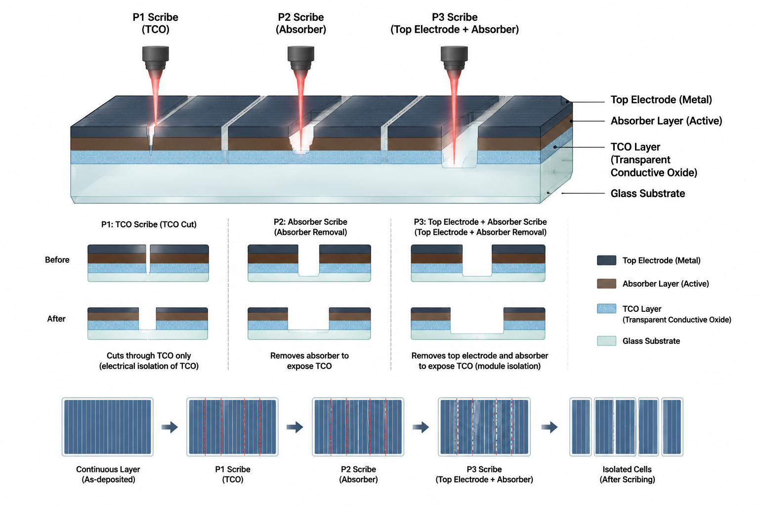
A single meter‑sized solar panel contains a continuous film stack. To generate usable electrical power, this large area must be divided into narrow photovoltaic cells that are connected in series. This series connection is achieved through three distinct laser scribing steps, known in the industry as P1, P2, and P3.
| Scribing Step | Purpose | Location |
|---|---|---|
| P1 | First scribe – isolates the bottom electrode (TCO) | Through the transparent conductive oxide (TCO) layer. |
| P2 | Second scribe – connects the top and bottom electrodes | Through the absorber layer to expose the bottom TCO. |
| P3 | Third scribe – isolates adjacent cells | Through the top electrode and absorber to the bottom TCO. |

2. The Principles of Laser Scribing
2.1 How Laser Scribing Works
Laser scribing uses a high‑energy laser beam focused onto the surface of the workpiece. The energy absorbed by the material causes localised melting and vaporisation, creating a narrow groove or scribe line. By precisely controlling the laser parameters—power, focus position, scanning speed, and pulse repetition rate—the scribe depth and width can be accurately controlled.
2.2 Why Laser for Solar Scribing?
Laser processing offers several critical advantages for photovoltaic scribing:
| Advantage | Why It Matters for Solar Cells |
|---|---|
| Non-contact processing | No mechanical stress—prevents cracking of fragile silicon or thin‑film structures. |
| Very small focused spot | Enables extremely fine, precise scribe lines—minimises dead area. |
| Short interaction time | Minimal heat‑affected zone (HAZ)—prevents thermal damage to adjacent layers. |
| Controlled depth | 2–3× depth control—enables precise removal of specific layers without damaging underlying films. |
| High speed | Increases throughput—essential for high‑volume manufacturing. |
| Suitable for coated substrates | Can scribe through protective or functional coatings. |
| Automation compatibility | Easily integrated into automated production lines. |
3. Thin‑Film Solar Cell Structure
Before understanding the scribing steps, it is useful to recall the typical structure of a thin‑film solar cell:
| Layer | Material | Function | Thickness |
|---|---|---|---|
| Substrate | Glass or flexible polymer | Provides mechanical support and optical transparency. | 1–3 mm |
| TCO (Transparent Conductive Oxide) | ITO, ZnO, FTO | Collects and transports electrons; transmits light to the absorber. | 0.5–2 µm |
| Absorber (Active Layer) | a‑Si, CdTe, CIGS, Perovskite | Converts light into electrical charge carriers. | 0.5–3 µm |
| Top Electrode | Metal (Al, Ag, Mo) or TCO | Collects holes and completes the electrical circuit. | 0.5–2 µm |
The challenge: To form a series‑connected module, the laser must selectively remove specific layers without damaging adjacent layers—a task that requires precise control of laser wavelength, pulse duration, and depth.

4. The Three Scribing Steps – P1, P2, and P3
4.1 P1 Scribing – Isolation of the Bottom TCO Layer
Purpose: P1 is the first laser scribing step performed during cell fabrication. It creates a groove through the bottom TCO layer, isolating the bottom electrode of one cell from the next. This prevents electrical short circuits between adjacent cells.
Process details:
| Aspect | Description |
|---|---|
| When performed | After the TCO layer is deposited and before the absorber layer is deposited. |
| Layer removed | Transparent Conductive Oxide (TCO) layer only. |
| Purpose | Electrically isolate the bottom electrode of each cell. |
| Scribe depth | 0.5–2 µm (must not penetrate the glass substrate). |
| Scribe width | Typically 30–50 µm. |
| Quality requirement | Complete removal of the TCO layer; no residual conductive material; no damage to the glass substrate. |
Why P1 matters: If the P1 scribe does not completely remove the TCO layer, the bottom electrodes of adjacent cells remain connected, creating a shunt path that reduces module efficiency. Conversely, if the scribe penetrates too deeply into the glass, it can create stress points and cause substrate cracking.
4.2 P2 Scribing – Series Connection of Electrodes
Purpose: P2 is the second scribing step. It removes the absorber layer (and optionally the top electrode) to expose the bottom TCO layer, allowing the top electrode of one cell to contact the bottom electrode of the adjacent cell. This creates the series electrical connection between cells.
Process details:
| Aspect | Description |
|---|---|
| When performed | After the absorber layer is deposited, before the top electrode is deposited. |
| Layer removed | Absorber layer (and optionally intermediate layers) to expose the bottom TCO. |
| Purpose | Create a contact window for series connection. |
| Scribe depth | Must expose the TCO layer without damaging it. |
| Scribe width | Typically 30–80 µm. |
| Quality requirement | Clean exposure of TCO; no residual absorber material; TCO surface must be conductive and ready for subsequent deposition. |
Why P2 matters: The P2 scribe is the critical connection point between cells. If the TCO is not fully exposed, the electrical contact resistance is high, reducing module efficiency. If the scribe penetrates too deeply, it damages the TCO, causing a poor electrical contact.
4.3 P3 Scribing – Isolation of Adjacent Cells
Purpose: P3 is the third and final scribing step. It removes the top electrode and the absorber layer down to the bottom TCO layer, electrically isolating adjacent cells from each other. This prevents current from flowing sideways and ensures that each cell operates independently.
Process details:
| Aspect | Description |
|---|---|
| When performed | After the top electrode is deposited. |
| Layer removed | Top electrode + absorber (down to the bottom TCO). |
| Purpose | Electrically isolate adjacent cells to prevent leakage. |
| Scribe depth | Through top electrode and absorber, stopping on the bottom TCO. |
| Scribe width | Typically 30–50 µm. |
| Quality requirement | Complete removal of top electrode and absorber; no damage to the bottom TCO; no residual conductive material that could cause short circuits. |
Why P3 matters: The P3 scribe defines the active area of each cell. If the scribe does not fully remove the top electrode, adjacent cells remain electrically connected, reducing module voltage and causing leakage current. If the scribe penetrates the bottom TCO, it can create a shunt path that reduces efficiency.
5. Chanxan Laser Scribing Solutions for Photovoltaics
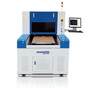
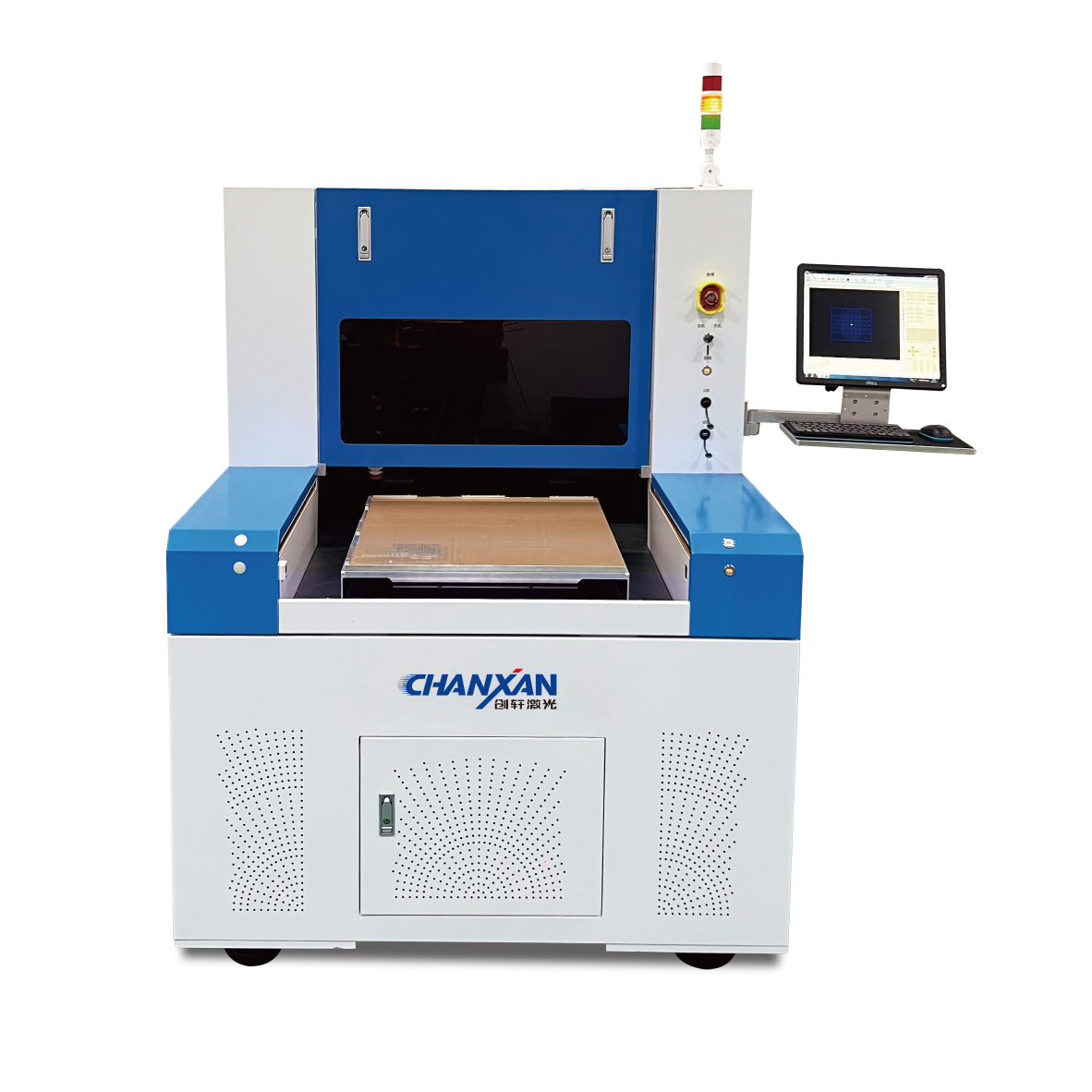
Chanxan Laser provides high‑precision laser scribing solutions for the photovoltaic industry, helping manufacturers achieve the quality, throughput, and yield required for competitive solar module production.
| Feature | Chanxan PV Laser Scribing System |
|---|---|
| Laser source | Picosecond/Femtosecond lasers – ideal for TCO and absorber materials; stable output; long service life |
| Focus control | Autofocus system for maintaining consistent scribe depth |
| Motion system | High‑precision XY stage with granite base for vibration‑free operation |
| Scribing precision | High positioning accuracy and repeatability |
| Software | User‑friendly interface; supports multiple scribing patterns; automated calibration |
| Processing speed | High – suitable for high‑volume production |
| Yield | High – minimal substrate damage and breakage |