Key Words: Silicon Wafer Dicing PCB Depaneling Glass Cutting
Home > Products > Laser Micromachining Systems
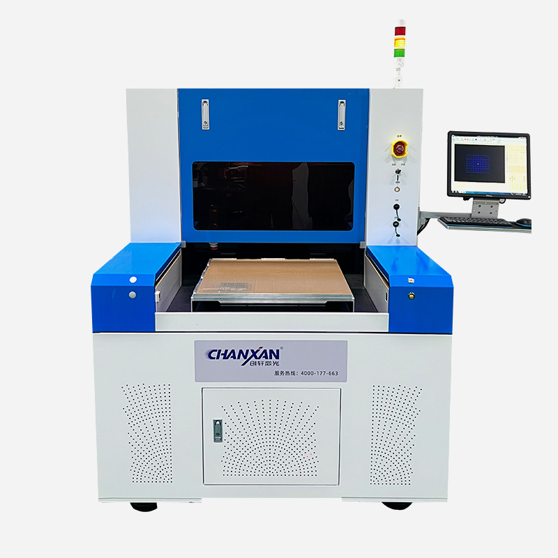
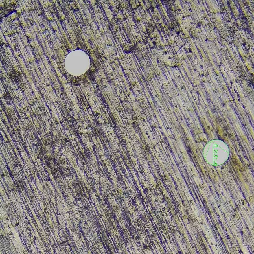
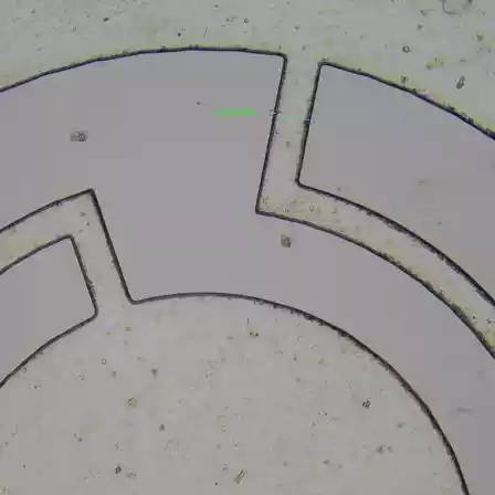
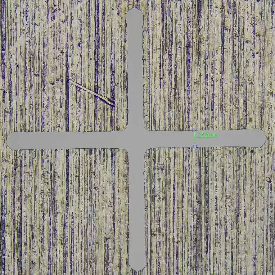
ITO laser patterning, touch panel manufacturing, Micro LED, transparent conductive film, ITO-coated glass
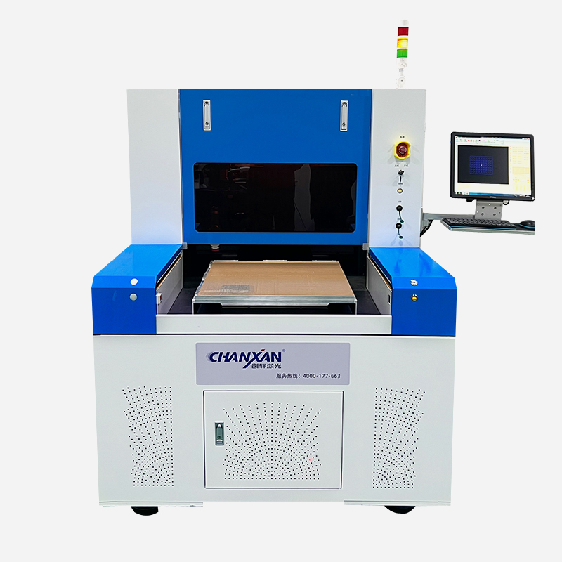
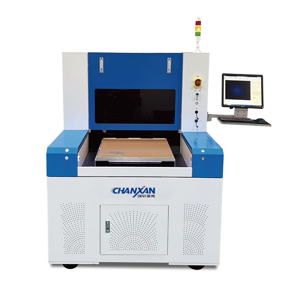
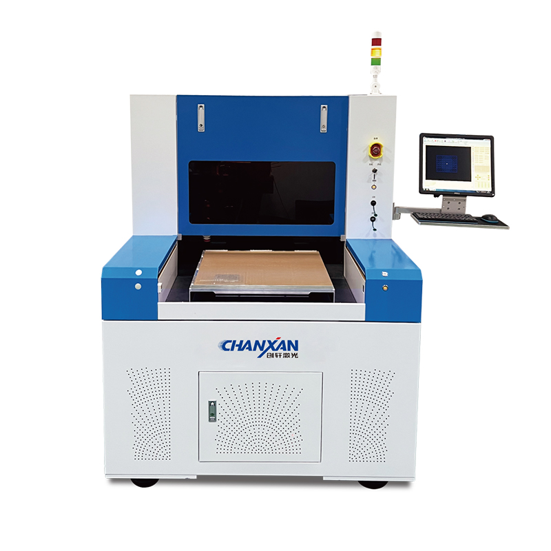
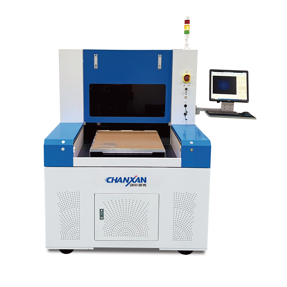
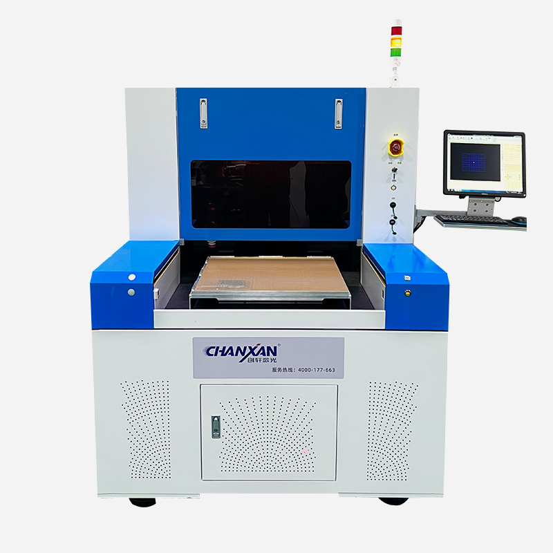
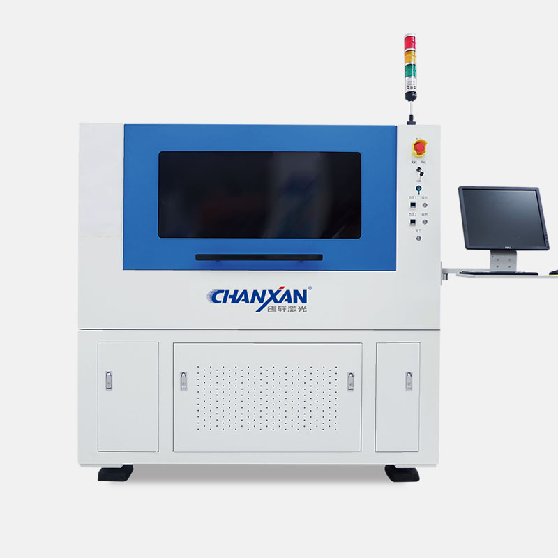
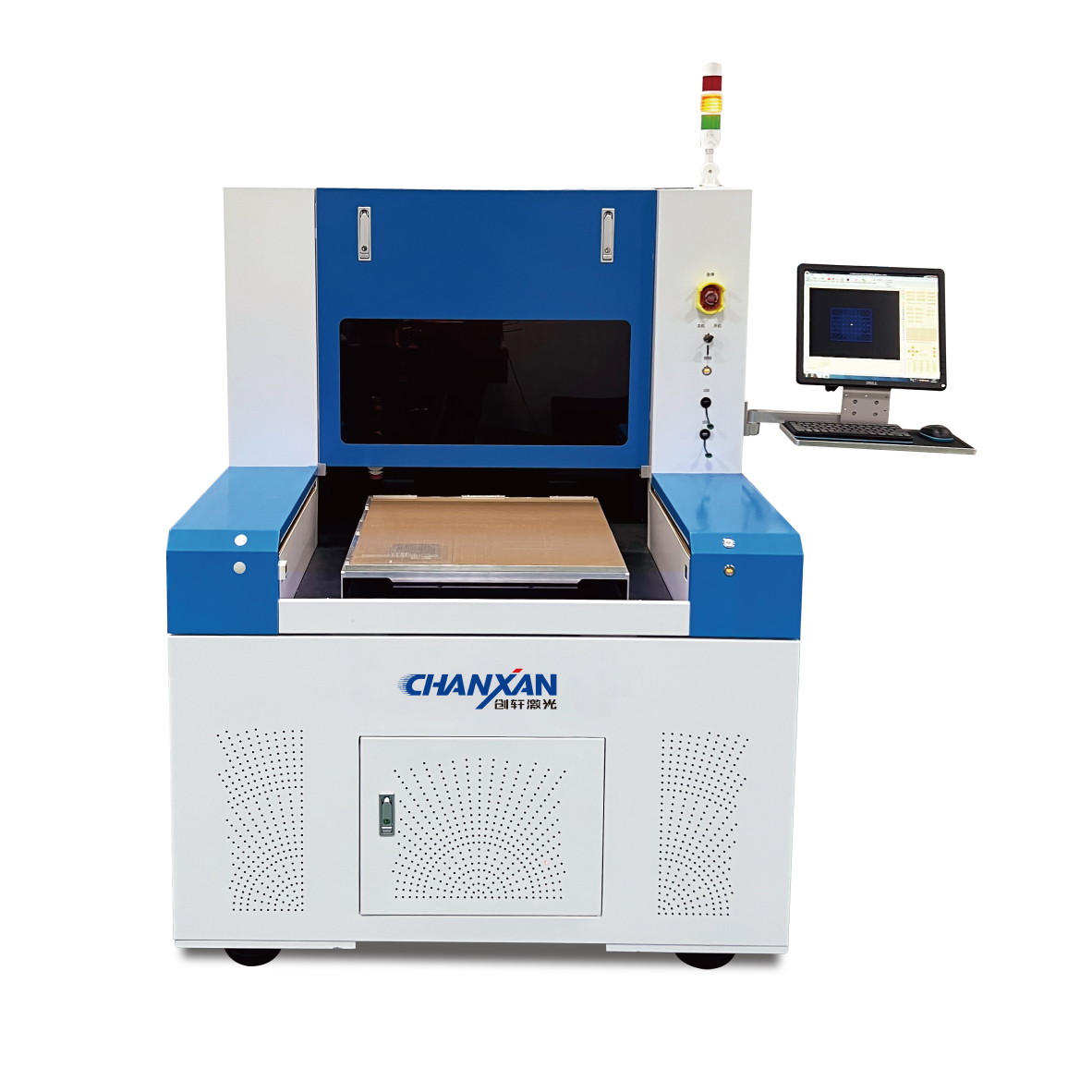
The Chanxan Picosecond Laser System is engineered for ultra-precise ITO (Indium Tin Oxide) patterning, transparent conductive film etching, and high-resolution micro-electrode structuring. Designed for advanced display and optoelectronic manufacturing, the system delivers true cold processing via ultrashort picosecond pulses, enabling damage-free removal of conductive films on glass and flexible substrates while maintaining excellent edge quality and electrical isolation. It is widely used in touch panels, OLED displays, Micro LED, and advanced transparent electrode fabrication.
ITO patterning is a critical manufacturing step in transparent electronics, used to define conductive circuits on glass or flexible substrates. The CW-6050PZ achieves this through non-thermal laser ablation, where ultrashort pulses directly break material bonds without excessive heat diffusion. Precise removal of ITO thin films, high optical transparency preservation in non-patterned areas, zero damage to glass or polymer substrates, and sub-micron edge control for high-density electrode layouts.
Superior edge quality with minimal thermal effects
Zero micro-cracking on glass substrates
Ultra-clean ITO removal without residue or redeposition
±1μm positioning accuracy for high-resolution patterns
Ideal for high-end display and semiconductor applications
Stable mass production capability with minimal drift
Cost-efficient solution for standard ITO patterning
Higher throughput for volume production
Potential thermal stress on sensitive substrates
Edge burning and residue issues on fine patterns
Limited precision for high-density electrode layouts
Suitable for applications with relaxed tolerance requirements
Precise ablation of ITO layers (10–200 nm) without substrate damage
Ultra-fine electrode pattern formation with ±1μm accuracy
Selective removal of conductive layers for complex circuit design
Sub-micron edge precision for high-density layouts
Maintains optical transparency in non-patterned areas
Up to 3000 mm/s engraving speed for mass production
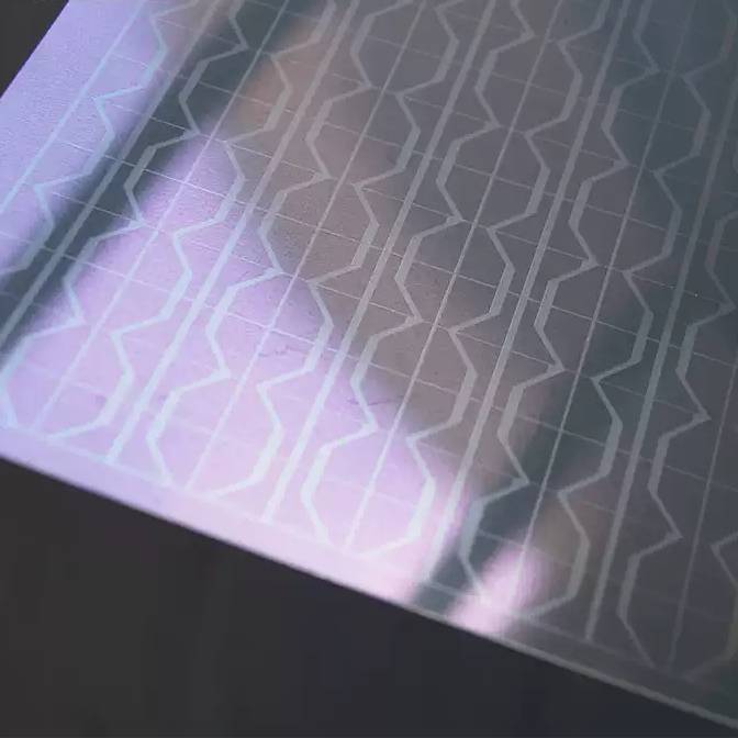
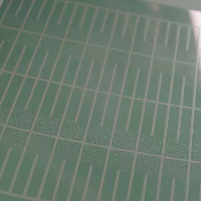
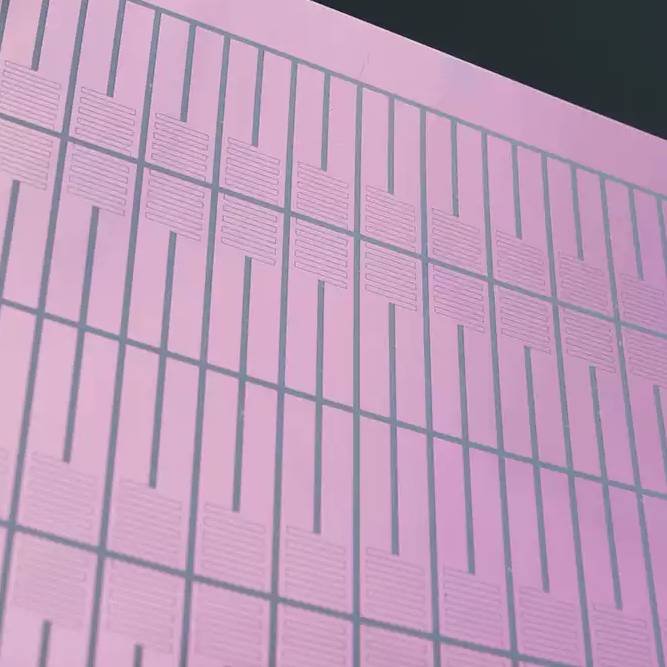
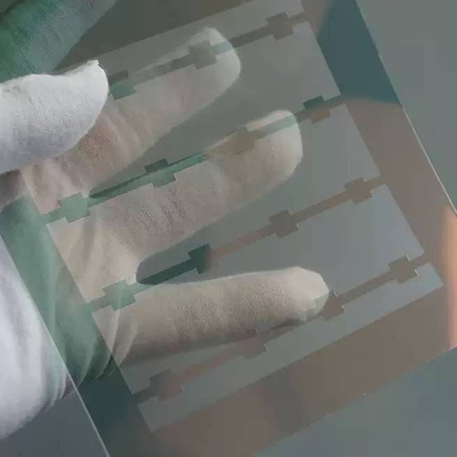
The CW-6050PZ is engineered for precision ITO patterning across diverse high-tech manufacturing sectors, from consumer electronics to advanced optoelectronic devices.
LCD / OLED electrode patterning
Transparent pixel structure formation
High-resolution display panel fabrication
Capacitive touch sensor electrode structuring
ITO grid patterning for smartphone screens
Large-area touch glass processing
Micro LED electrode fabrication
Transparent circuit design for AR/VR devices
Flexible transparent conductive circuits
Thin film conductive layer structuring
Transparent material micro-processing
Advanced functional coating patterning
Ultrashort pulse laser delivers high peak power with minimal thermal diffusion, enabling precise ITO film ablation without damaging glass substrates.
Ensures stable, vibration-free motion for micron-level precision during high-speed patterning.
Automatically detects substrate alignment marks for precise registration of complex electrode patterns.
Industrial-grade granite platform ensures long-term mechanical stability and vibration suppression.
Picosecond laser pulses eliminate thermal stress on glass substrates, preventing micro-cracks and ensuring high yield in display manufacturing.
The system enables precise removal of ITO layers without residue, redeposition, or edge burning, ensuring high electrical isolation performance.
With ±1μm positioning accuracy and CCD vision alignment, the system supports ultra-fine electrode patterns for high-resolution display and touch applications.
Designed for industrial-scale production lines, ensuring consistent pattern quality across long runs with minimal drift or deviation.
| Item | Specification |
|---|---|
| Model | CW-6050PZ |
| Laser Type | Picosecond UV / IR / Green |
| Laser Power | 30W |
| Working Area | 500 × 500 mm / 600 × 900 mm |
| Adsorption Platform | 1200 × 700 mm (customizable) |
| Positioning Accuracy | ±1 μm |
| Repeatability | ±1 μm |
| Machining Accuracy | ≤30 μm |
| Machining Speed | ≤3000 mm/s |
| Machining Thickness | ≤3 mm |
| Motion System | X/Y/Z Three-Axis Linear Motor System |
| Vision System | High-Resolution CCD Alignment |
| Control Software | Chanxan Self-Developed System |
| Supported Formats | PLT, BMP, DXF, DWG, AI, LAS |
| Power Supply | 380V ±10%, 50Hz |
Empowering global manufacturing with 14+ years of expertise, dual CE & ISO certified quality, over 100 national patents, and a comprehensive Technical Training Service designed for your operational success.
Systematic Training: Comprehensive full-process skill coverage.
Expert Support: Continuous project follow-up by senior engineers.
Multiple Formats: Flexible learning modes to maximize operational efficiency.
Outcome Driven: Empowering clients from "knowing" to "mastering" technology.
24H Fast Response: Technical diagnosis and solutions within 24 hours.
Warranty Policy: 1-year machine warranty with lifetime technical support.
Global Parts Supply: Rapid delivery of original parts via global network.
Lifecycle Care: From installation to long-term maintenance and software upgrades.
In-depth analysis of your specific material and performance requirements.
Precision laser sampling to verify the feasibility of the technical solution.
Bespoke manufacturing under ISO9001 quality management systems.
Final testing, professional wooden packing, and secure global shipment.
We are seeking professional partners to expand our presence in the global industrial laser market. Scale your business with Chanxan's high-end technology and manufacturing strength.
Become an AgentApplications
Subscriber:Picosecond ITO Patterning Laser System