Key Words: Silicon Wafer Dicing PCB Depaneling Glass Cutting
Home > News > Industry News
【Description】:
Master LCP laser processing without thermal melt flow. Discover ultra-short pulse laser solutions for clean microvias and damage-free 5G mmWave substrates.
Liquid crystal polymer (LCP) owes its irreplaceable position in 5G mmWave modules to its unique molecular structure: even after solidification, its rigid, rod-like molecular chains maintain a highly oriented alignment. This distinct molecular arrangement grants LCP exceptional dielectric stability from microwave to terahertz frequencies, alongside excellent low moisture absorption.
However, this thermoplastic structure simultaneously introduces a highly demanding thermal challenge during processing:
Traditional Substrates (e.g., PI): When exposed to excessive heat, polyimide primarily degrades and chars, maintaining a relatively stable structural boundary.
LCP Materials: LCP has a significantly low melting point and exhibits classic thermoplastic behavior—it melts and flows immediately upon reaching its melting temperature.
Consequently, LCP operates within a much tighter process window than PI. In any thermal-based processing (such as laser cutting or drilling), even a minor lingering of heat causes the material edges to melt and deform, demanding extremely strict control over total heat input.
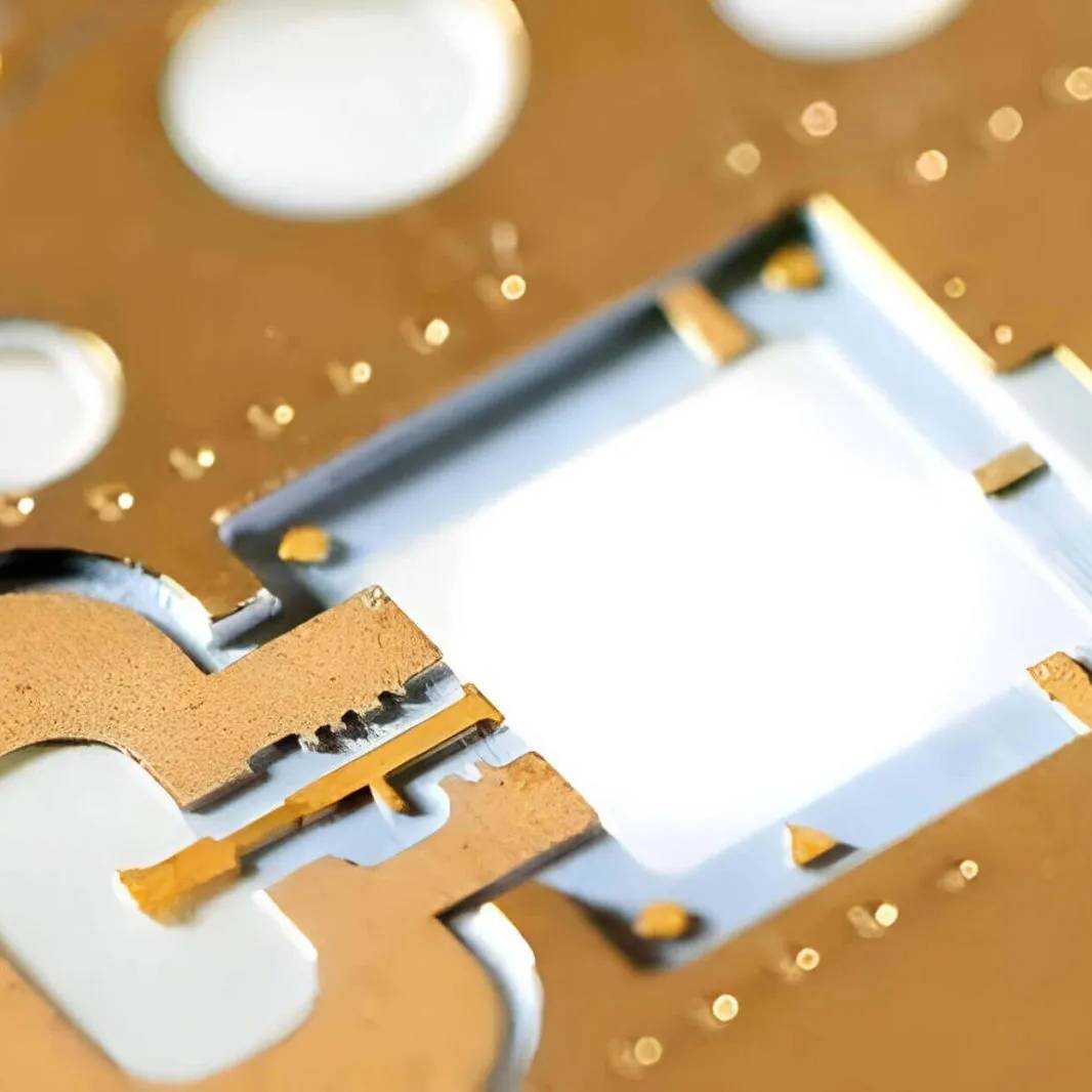
LCP bondply melts at approximately 290°C, meaning multilayer constructions are strictly designed around the limitation that the material can only tolerate brief, momentary exposures near that temperature threshold. In contrast, polyimide (PI) lacks a true melting point under standard processing conditions, successfully resisting thermal degradation well past 400°C.
This thermal gap of roughly 100–150°C completely redefines the consequences of "excessive heat input" in production:
On Polyimide (PI): Excess laser dwell time typically results in manageable, marginal carbonization (charring) along the edges.
On Liquid Crystal Polymer (LCP): Excess heat causes immediate softening and material flow. In practice, this fluid failure mode distorts via walls, blurs precision coverlay openings, and—in complex multilayer stacks—directly compromises the critical bond between the LCP layers and copper foil.
While standard nanosecond UV laser drilling is already the established baseline for multilayer LCP via formation, ultra-short picosecond and femtosecond pulses introduce a critical processing advantage: they remove material before significant thermal energy can conduct into the surrounding substrate and trigger melt-flow failure.
Because the pulse duration is exceptionally brief—on the scale of picoseconds or femtoseconds—the material ejection occurs faster than the rate of thermal conduction into the adjacent LCP matrix.
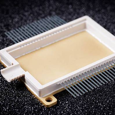
Pristine Microvia Sidewalls: Eliminates the formation of melt-extruded ridges or lips at the bottom of the via.
Sharper Coverlay Geometry: Yields crisp, distinct coverlay window edges with zero thermal recession.
Preserved Layer Adhesion: Drastically mitigates the risk of delamination, protecting the critical LCP–copper bond during high-density, repetitive via drilling across complex multilayer panels.
| Process | Typical role on LCP | Thermal margin used | Best fit |
|---|---|---|---|
| Mechanical drilling | Larger through-vias, low layer count | None — can deform LCP under poor parameters | Simple, low-density structures |
| UV nanosecond | Established baseline for multilayer microvia drilling | Moderate — controlled but still thermal | General multilayer LCP via formation |
| Picosecond | Fine-pitch microvias, antenna trim, mmWave AiP modules | Low — faster than melt-flow can develop | Tight-pitch, high-reliability work |
| Femtosecond | Most heat-sensitive multilayer stacks, R&D | Minimal | Highest-margin work, lower throughput |
Antenna-in-Package (AiP) — fine interlayer vias on multilayer LCP stacks for mmWave antenna modules.
High-Frequency Flex — drilling and trimming on LCP flex circuits operating from microwave into terahertz frequencies.
Fine-Pitch FPC — opening coverlay windows on LCP-based FPC without melt-flow disturbing the adjacent dielectric.
Precision Trim — trimming copper antenna geometry on LCP substrate without softening the dielectric beneath the trace.
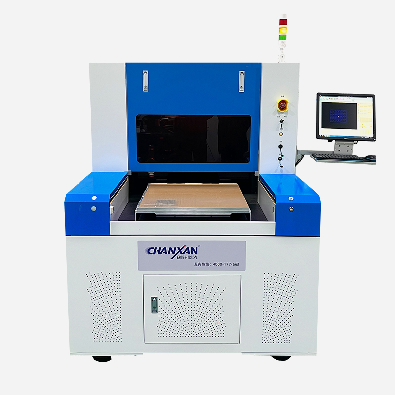
The CW-6050PZ picosecond laser system is a highly versatile, industrial-grade ultrafast laser system engineered to handle the industry's most challenging high-frequency and optoelectronic substrates.
For 5G mmWave LCP Processing: Configured with a UV source, the CW-6050PZ delivers the ultra-short pulse durations necessary to "outrun" thermal conduction. By removing material before it reaches the critical 290°C melt-flow regime, it yields pristine microvia sidewalls without extruded lips and prevents delamination of the sensitive LCP-to-copper bond.
For Optoelectronic ITO Patterning: Configured with a 1064 nm IR source, the system leverages the massive "order-of-magnitude" ablation threshold gap between the ITO film (0.07 J/cm²) and underlying glass or PET substrates, achieving flawless selective scribing with zero distortion to the backing material.
Every production line scales differently. For manufacturing facilities where a configurable multi-wavelength system exceeds project scope, ChanXan's broader ultrafast laser platform family includes dedicated, single-purpose Nanosecond and Femtosecond machines. Whether you require cost-effective baseline drilling or absolute sub-micron cold processing, ChanXan provides a tailored configuration to maximize your yield and ROI.
| Free solution
Previous: Precision Laser Direct-Write (LDW) for ITO Film Patterning
Next: Polypropylene (PP) Laser Cutting | CO2, UV & Ultrafast Laser Processing Solutions