Key Words: Silicon Wafer Dicing PCB Depaneling Glass Cutting
Home > News > Industry News
【Description】:
Discover the challenges of LCP film laser cutting. Learn how ultrashort pulse (USP) lasers eliminate HAZ and carbonization for high-yield FPC production.
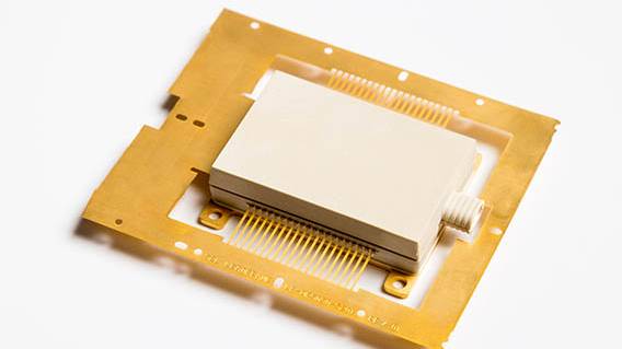
With the rapid expansion of 5G/6G high-frequency communications, millimeter-wave radar, and advanced medical electronics, LCP (Liquid Crystal Polymer) films have emerged as the next-generation substrate for flexible printed circuits (FPCs). Valued for their near-zero dielectric loss (low Df/Dk), exceptional moisture resistance, and high dimensional stability, LCP films are quickly replacing traditional polyimide (PI) in high-end applications.
However, for procurement managers and production engineers, transitioning to LCP brings major manufacturing hurdles. Its unique molecular structure makes it notoriously difficult to process using mechanical die-cutting or legacy laser systems. Achieving high-yield, cost-effective LCP film laser cutting has become a critical milestone for electronics manufacturers looking to optimize their production return on investment (ROI).
Before evaluating equipment or making a purchasing decision, it is essential to understand the core technical pain points of LCP thin film processing:
LCP is a thermoplastic polymer with highly oriented molecular chains. While it has excellent thermal stability, it is extremely sensitive to prolonged thermal exposure. When processed with traditional CO2 lasers or standard nanosecond UV lasers, the long pulse width creates a broad heat-affected zone (HAZ). This results in edge melting, thermal deformation (warping), and severe carbonization (charring) along the cut line, which compromises the electrical insulation of the circuit.
Due to its liquid crystal nature, LCP exhibit significant anisotropy—meaning its mechanical properties differ depending on the direction of the material flow. Mechanical die-cutting often causes micro-tearing, delamination, and rough edges. Meanwhile, thermal-heavy laser processing can amplify these structural discrepancies, leading to inconsistent edge quality across the X and Y axes.
Modern FPCs require high-density interconnects (HDI) with sub-50-micron microvias. Controlling the taper angle and eliminating residual resin or debris inside these micro-holes is incredibly difficult without the right laser wavelengths and pulse durations.
To overcome these barriers and secure a competitive edge in high-volume production, the industry has shifted from thermal-based cutting to ultrashort pulse (USP) laser cold processing, utilizing picosecond and femtosecond lasers.
| Feature / Metric | Nanosecond UV Laser | Picosecond / Femtosecond Laser |
|---|---|---|
| Processing Mechanism | Photothermal (Melting/Burning) | Photoablation (Direct Bond Breaking) |
| Heat-Affected Zone (HAZ) | <50 um(High risk of warping) | <10 um (Near-zero thermal impact) |
| Edge Quality | Visible charring, requires post-cleaning | Carbonization-free, smooth edge profile |
| Precision & Repeatability | Moderate | Ultra-high (± 2 μm accuracy) |
Photoablation over Melting: Picosecond and femtosecond lasers deliver peak power in bursts so incredibly fast that they break the molecular bonds of the LCP material instantly. The material vaporizes before heat can conduct to the surrounding areas, achieving carbonization-free FPC cutting.
Eliminating Post-Processing Costs: Because the edge quality is clean and free of debris, manufacturers can bypass expensive, time-consuming chemical cleaning steps, directly boosting throughput and yield rates.
When sourcing an industrial laser system for LCP film or flexible PCB manufacturing, your evaluation checklist should focus on the following parameters:
Wavelength and Pulse Width: For thin films, a green or UV picosecond/femtosecond laser yields the cleanest ablation.
Optical Beam Shaping: Advanced optical setups—such as transforming a standard Gaussian beam into a top-hat profile—distribute laser energy evenly, further minimizing the taper angle in micro-drilling.
Handling System Integration: For high-volume manufacturing, look for automated material handling, such as Roll-to-Roll (R2R) laser cutting configurations, to reduce manual labor costs and prevent material deformation during loading.
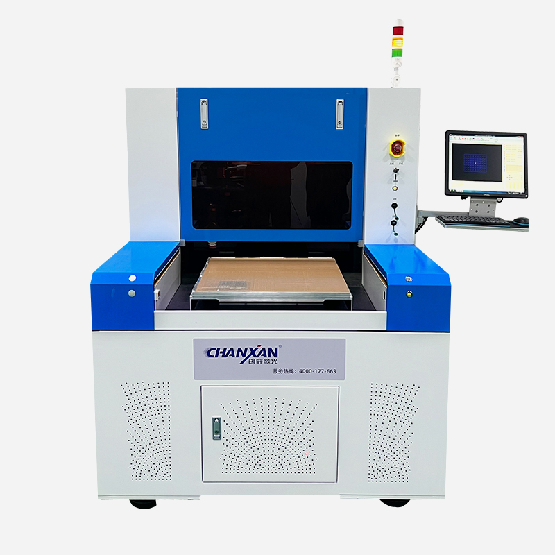
To meet the rigorous standards of high-frequency flexible electronics, Chanxan Laser has engineered a state-of-the-art series of high-precision industrial laser equipment specifically optimized for micro-cutting and micro-drilling advanced polymer substrates.
Ultra-Short Pulse Performance: Equipped with premium picosecond and femtosecond laser engines, Chanxan's platforms achieve a heat-affected zone of less than 3 um, eliminating edge yellowing, melting, and carbonization on LCP, PI, and LCP-Coverlay composites.
Industrial-Grade Precision: Integrated with high-resolution vision alignment systems and linear motor drives, our platforms deliver an absolute cutting accuracy of 2 um, making them ideal for the tightest semiconductor and automotive electronics tolerances.
Versatile Application Spectrum: Designed to seamlessly process everything from LCP and LCP/PI multi-layer boards to copper-clad laminates (CCL) and rigid-flex PCBs, offering flexible manufacturers a future-proof investment.
B2B Customization & R2R Readiness: We understand that every production line is unique. Chanxan provides tailormade beam shaping options, automated sheet-fed handlers, and full roll-to-roll integrations designed to maximize your throughput and minimize your total cost of ownership (TCO).
Don't let legacy thermal cutting methods hold back your product quality or compromise your material yields. Reach out to our application engineering team today to request a free sample cutting trial on your LCP substrates and discover how our ultrafast laser technology can optimize your manufacturing ROI.
| Free solution
Previous: Precision Laser Patterning for ITO Films in Touch Screen Manufacturing
Next: Picosecond Laser Cutting for Flexible PCBs: Minimizing HAZ and Carbonization