Key Words: Silicon Wafer Dicing PCB Depaneling Glass Cutting
Home > News > Industry News
【Description】:
Discover how picosecond selective laser ablation achieves invisible ITO film patterning for touch screen manufacturing without PET substrate damage. Optimize your production ROI.
In the high-stakes world of touch screen panels, capacitive sensors, and flexible displays, Indium Tin Oxide (ITO) remains the dominant transparent conductive oxide (TCO) material. To form the intricate electrode arrays required for modern multi-touch functionality, manufacturers must utilize selective ITO laser ablation. This process removes precise channels of the conductive layer while leaving the underlying substrate completely untouched.
However, as consumer demand shifts toward bezel-less designs, higher pixel densities, and ultra-flexible form factors, legacy processing methods are hitting a wall. Achieving cost-effective, high-yield, and optically flawless ITO laser patterning is now a primary focus for optoelectronic production engineers globally.
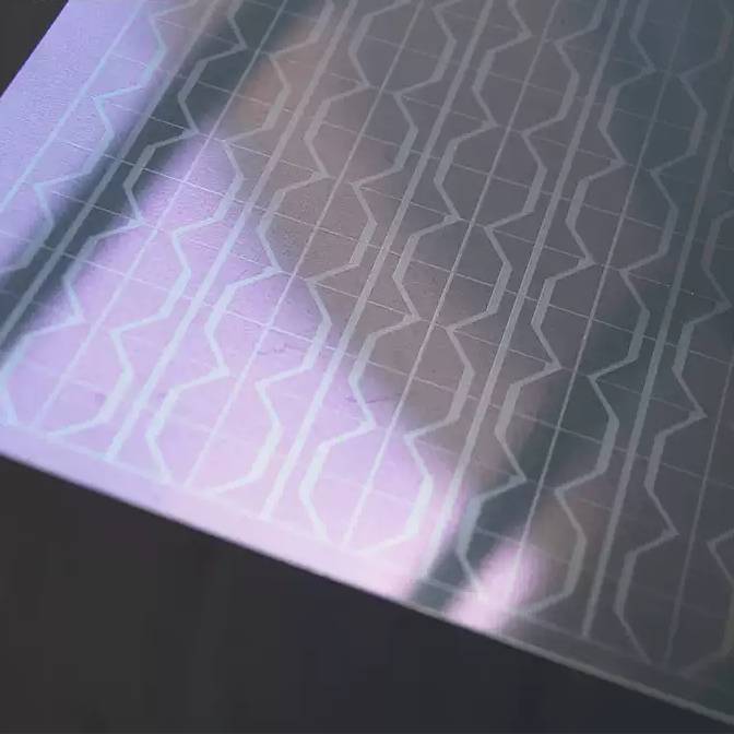
The core challenge of patterning ITO lies in the delicate relationship between the film and its backing material—typically flexible Polyethylene Terephthalate (PET) or ultra-thin glass. ITO coatings are incredibly thin, often ranging from 15 to 100 nanometers.
When engineering an automated production line, technical teams face a tight process window dictated by the material ablation thresholds:
The ITO Film: Possesses a relatively low ablation threshold (approximately 0.07 J/cm² under localized energy deployment).
The Underlying Substrate: While PET and glass have higher bulk thresholds, they are highly sensitive to thermal stress. Legacy nanosecond lasers generate a broad Heat-Affected Zone (HAZ), which conducts heat downward, causing the PET to melt, warp, or crack, leading to electrical shorts or structural failure along the etched tracks.
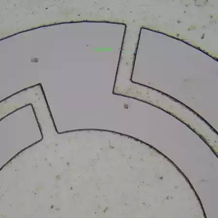
Beyond structural integrity, touch screen manufacturing demands strict optical uniformity. If a laser relies too heavily on photothermal degradation (melting), it creates microscopic ridges of re-deposited material at the track edges. These ridges cause an optical mismatch, making the laser-etched pattern visible to the naked eye under ambient light—a critical defect in premium smartphone or automotive displays.
To resolve this, advanced manufacturing lines utilize ultrashort pulse (USP) laser scribing. By compressing the laser energy into a picosecond time frame, the mechanism shifts from melting to pure photoablation. The laser breaks atomic bonds instantly, vaporizing the ITO film before thermal energy has time to propagate into the adjacent matrix or substrate, delivering true invisible laser patterning.
| Process Metric | Legacy Nanosecond Processing | Precision Picosecond Processing |
|---|---|---|
| Primary Mechanism | Photothermal (Melting / Boiling) | Photoablation (Cold Laser Processing) |
| Substrate Thermal Stress | High (Risk of PET micro-warping) | Zero (Substrate structure fully preserved) |
| Edge Ridge Formation | Significant (Creates visible reflection tracks) | Sub-micron clean boundaries (Invisible pattern) |
| Isolation Resistance | Inconsistent due to thermal debris | Ultra-high and stable (> 100 MΩ) |
Laser Fluence (J/cm²): Must be locked tightly above 0.07 J/cm² but strictly below the damage threshold of the PET/glass backing.
Pulse Overlap & Scan Speed: Inadequate overlap leaves conductive bridges, failing isolation tests. Excessive overlap accumulates residual heat, inducing micro-cracks in glass or melting in PET.
Wavelength Selection: While UV provides tight spot focuses, standard 1064 nm Infrared (IR) configurations leverage a massive order-of-magnitude threshold gap between the ITO film and glass, making IR exceptionally reliable for specific selective scribing configurations.
Engineered specifically to solve the yield, precision, and optical visibility challenges in modern optoelectronics manufacturing, the Chanxan CW-6050PZ Picosecond Laser System represents the peak of high-throughput industrial cold processing.
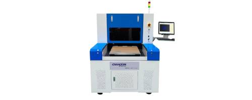
Exploiting the 0.07 J/cm² Threshold Gap: When configured with an industrial 1064 nm IR or 532 nm Green source, the CW-6050PZ perfectly balances energy delivery to effortlessly strip the micro-thin ITO conductive layer while remaining safely invisible to underlying glass or PET sheets.
Guaranteed Invisible Scribing: By delivering pulse widths in the precise picosecond domain, the platform completely eliminates edge melting, slag re-deposition, and thermal warping. The resulting isolation channels feature razor-sharp geometries that are entirely imperceptible to consumer end-users.
High-Speed Production Galvanometer: Equipped with premium, ultra-fast digital scanning galvo-heads and real-time vision alignment, the CW-6050PZ handles intricate capacitive matrix patterns at blazing speeds with an absolute accuracy of 2 um.
Scalable Multi-Material Versatility: Beyond basic ITO films, the Chanxan ultrafast platform scales effortlessly across your facility to handle ultra-thin glass cutting, flexible PCB coverlay window profiling, 5G LCP drilling, and silver paste trace line isolation.
Don't let scrap rates, micro-cracks, or visible etch marks impact your manufacturing margins. Contact Chanxan Laser's technical application group today to coordinate a free sample validation trial on your specific ITO-coated substrates and discover how our picosecond cold ablation technology can optimize your production ROI.
| Free solution
Previous: Picosecond Laser Direct Writing of Laser-Induced Graphene Electrodes on Polyimide Films
Next: Laser Cutting of LCP (Liquid Crystal Polymer) Films: Challenges and Solutions