Key Words: Silicon Wafer Dicing PCB Depaneling Glass Cutting
Home > News > Company News
【Description】:
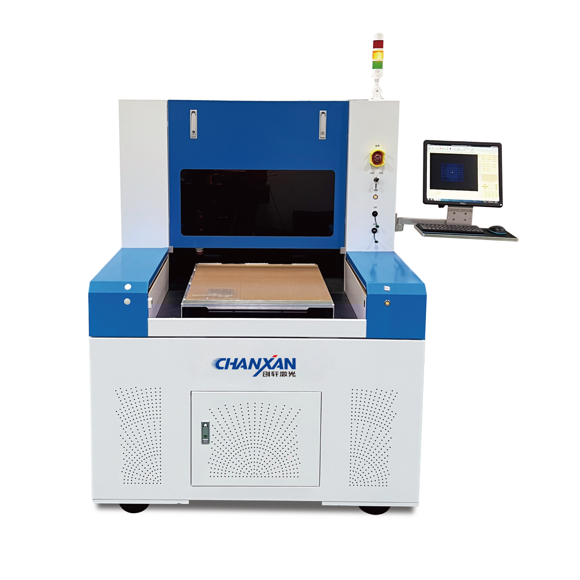
Chanxan CW-6050PZ automatic wafer laser marking system offers precision non-contact marking for 6/8/12-inch wafers. Maximize chip traceability at the DIE level.
As semiconductor devices continue their relentless march toward miniaturization, every stage of manufacturing must adapt—including individual die identification. Wafer laser marking has become a critical discipline. As chip dimensions shrink, traceability codes must compress in tandem, demanding absolute positioning accuracy.
Unlike marking large mechanical parts, a wafer marking system must place legible, permanent characters within highly constrained areas on dies just a few millimeters across—all without damaging surrounding circuitry or specialized coatings. Chanxan Laser delivers purpose-designed equipment to handle these strict beam performance requirements, even on highly sensitive coated wafers.
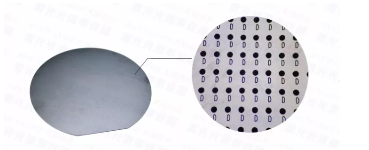
The Chanxan CW-6050PZ automatic wafer laser marking system is engineered to translate sub-micron requirements into high-throughput factory execution.
Wafer Size Flexibility: Full compatibility with 6-inch, 8-inch, and 12-inch wafers to prevent fabrication bottlenecks.
Input Format: Accepts incoming material seamlessly in standard cassette or box formats.
Granular Control: Precise markings executed directly at the individual DIE level.
Advanced Optics: Utilizes Green (532nm) or Ultraviolet (355nm) laser sources for optimized material absorption and ultra-small spot sizes.
Similar to advanced UV laser dicing solutions , the marking process is entirely non-contact. This eliminates physical stress, micro-fractures, and particle contamination on delicate substrates.
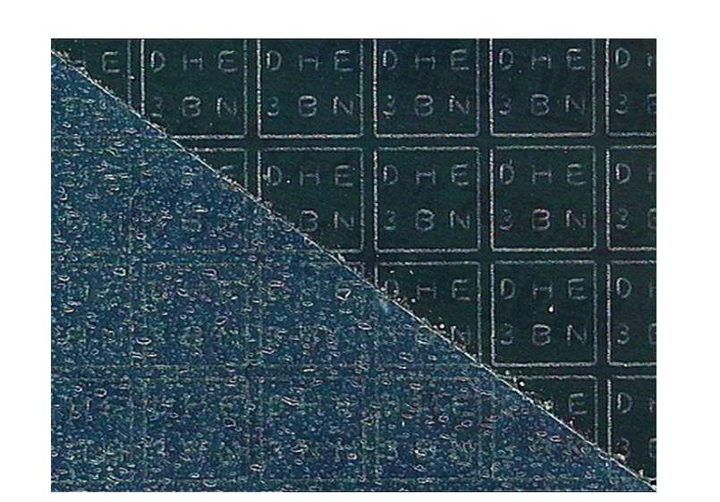
The platform runs on a computer-controlled Windows architecture with self-developed software, integrating full-scale automation across the mechanical structure:
| Integrated Feature | Industrial Production Benefit |
|---|---|
| Auto Loading/Unloading | Handles wafer transport without manual intervention to protect yield. |
| Visual Inspection CCD | Instantly verifies mark quality and micro-positioning placement accuracy. |
| Main Beam Lifting | Maintains strict focus consistency across varying wafer thicknesses. |
| Safety & Diagnostics | Integrated smoke exhaust system and automatic error alarms to avoid scrapped product. |
Wafer laser marking shares fundamental physics with the broader dicing ecosystem. Fabs already employing laser cutting for silicon and SiC wafers can naturally integrate the CW-6050PZ platform. Sharing similar beam-delivery paradigms and automation logic makes green and UV marking a seamless technical upgrade.
Figure: Chanxan CW-6050PZ delivers high-density automated marking solutions
| Free solution
Previous: blouse laser cutting machine