Key Words: Silicon Wafer Dicing PCB Depaneling Glass Cutting
Home > Products > Laser Micromachining Systems
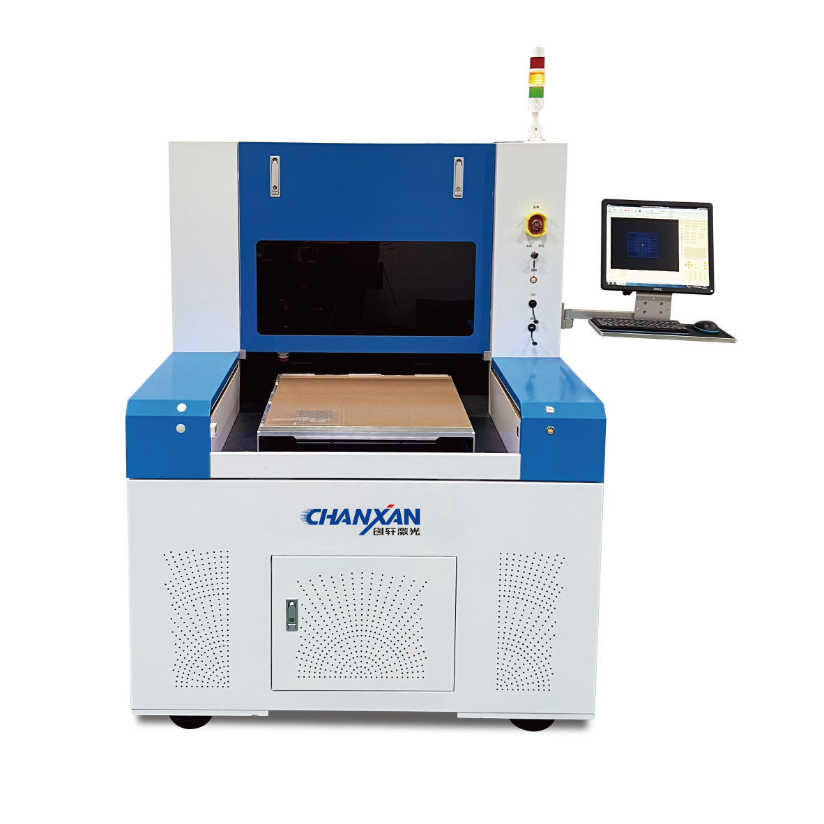

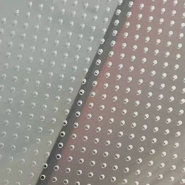
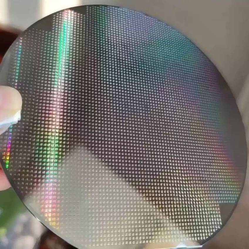
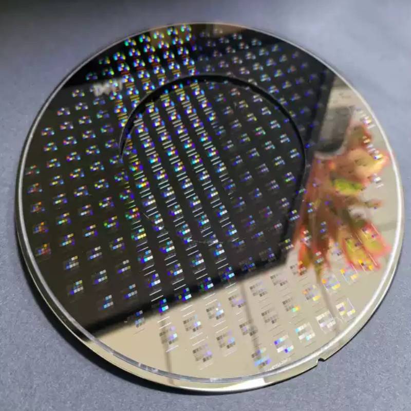
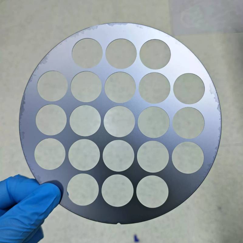
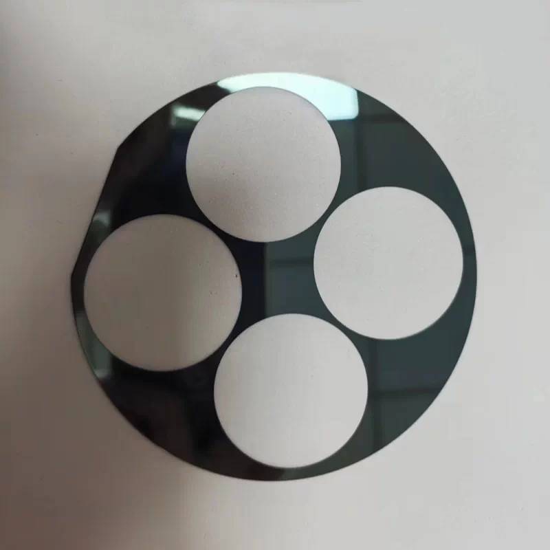
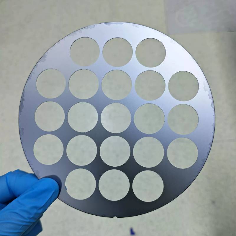
Silicon wafer, SiC, GaN, Sapphire wafer, Glass wafer, Ceramic wafer processing
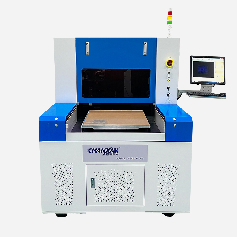
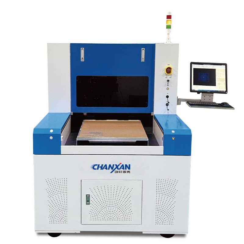
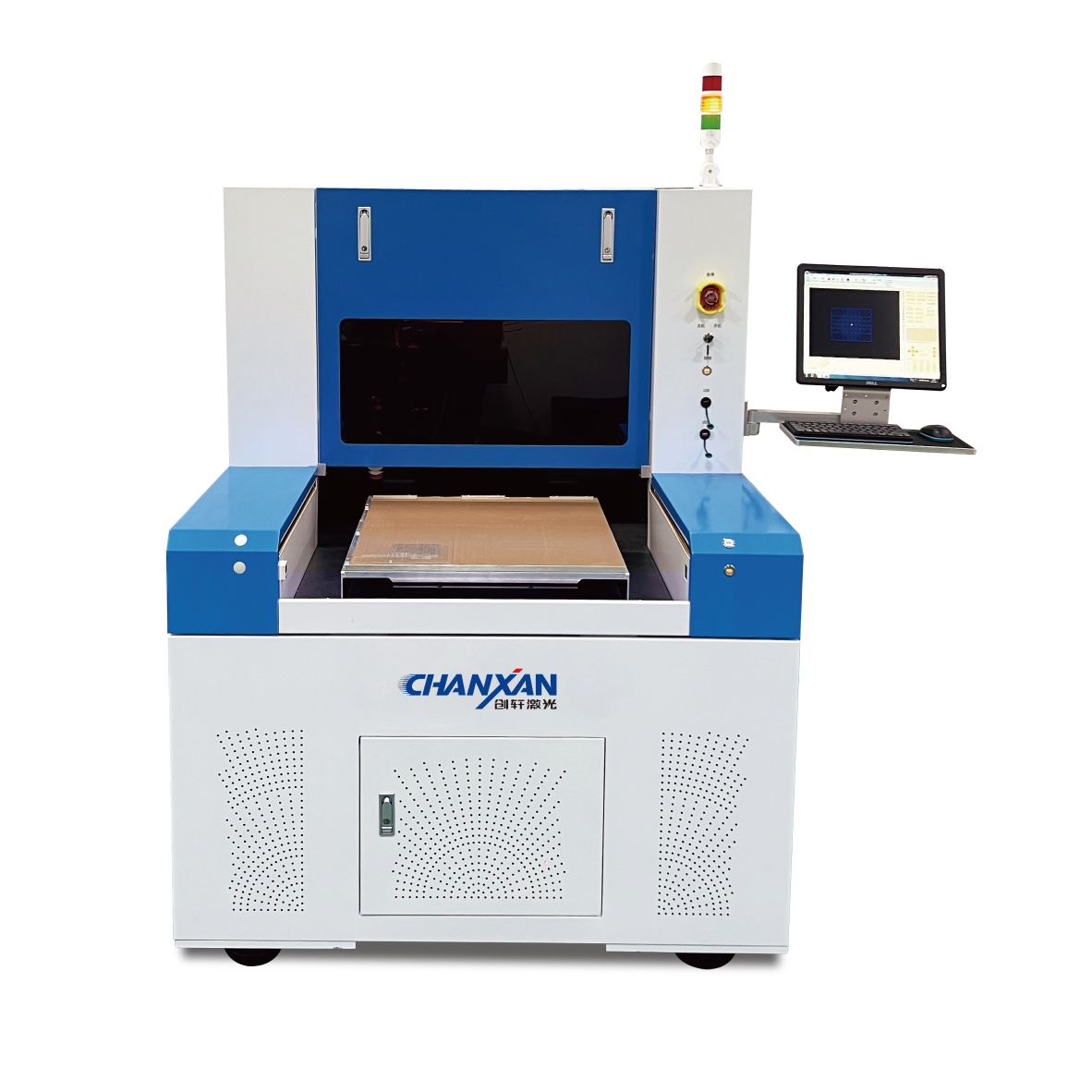
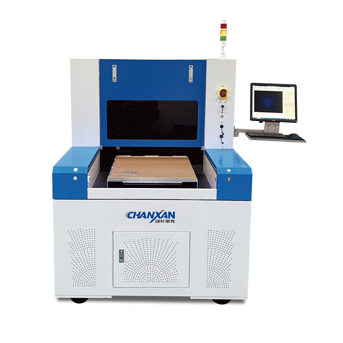
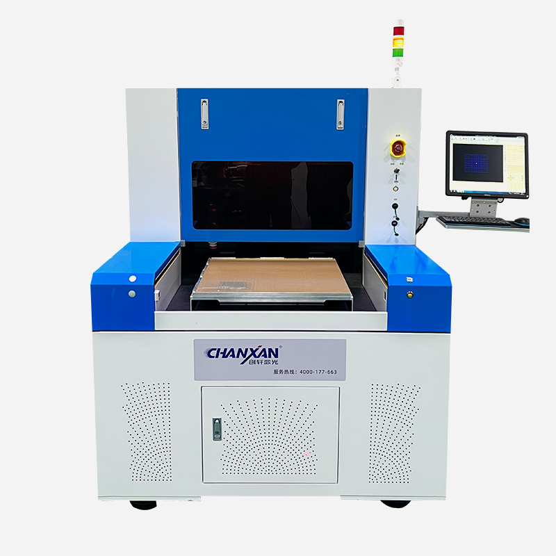
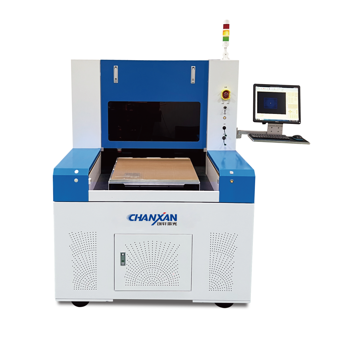
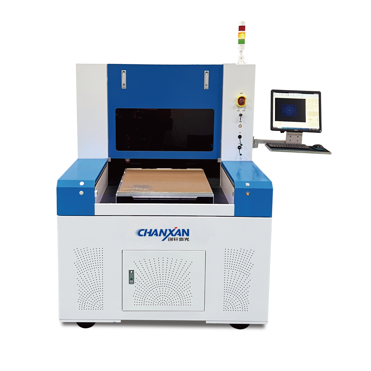
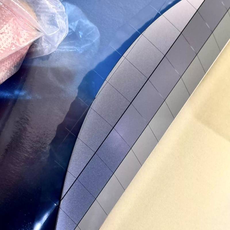
Designed for third-generation semiconductors, wafer-level packaging, MEMS, advanced substrates, and precision microelectronics, the Chanxan picosecond wafer dicing system delivers clean singulation paths, narrow streets, fine grooves, and low-damage edge quality across demanding semiconductor materials. Especially suitable for SiC wafers, GaN wafers, sapphire wafers, glass wafers, ceramic substrates, and wafer-level packaging structures.
Chanxan's picosecond wafer dicing laser cutting machine is designed around direct ablation cutting. In this process, the laser is focused onto the wafer surface and removes material by instantaneous high-energy-density ablation, forming a dicing trench or through-cut without mechanical blade contact. It is widely applicable to SiC, GaN, sapphire, glass, ceramic, and selected multilayer semiconductor wafer structures, as well as to laser grooving of advanced silicon wafers with fragile surface stacks.
Physical blade grinds through wafer
Severe blade wear on SiC, sapphire, and ceramics
High Chipping Risk on brittle wafers and hard substrates
Risk of delamination or tearing in hybrid stacks
Limited by blade geometry and process mechanics
Introduces cutting force and vibration
Laser removes material directly from the wafer surface through ultrafast ablation
Well suited to hard and brittle materials where blade wear is a major issue
Lower edge chipping with controlled ultrafast ablation
Better suited to metal + polymer + dielectric + substrate composite structures
Digital path control for fine grooves, narrow streets, and complex contours
Fully non-contact with no blade pressure on the wafer
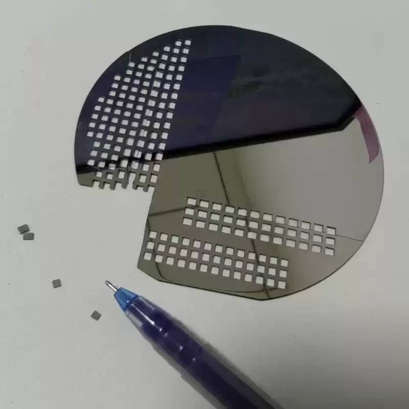
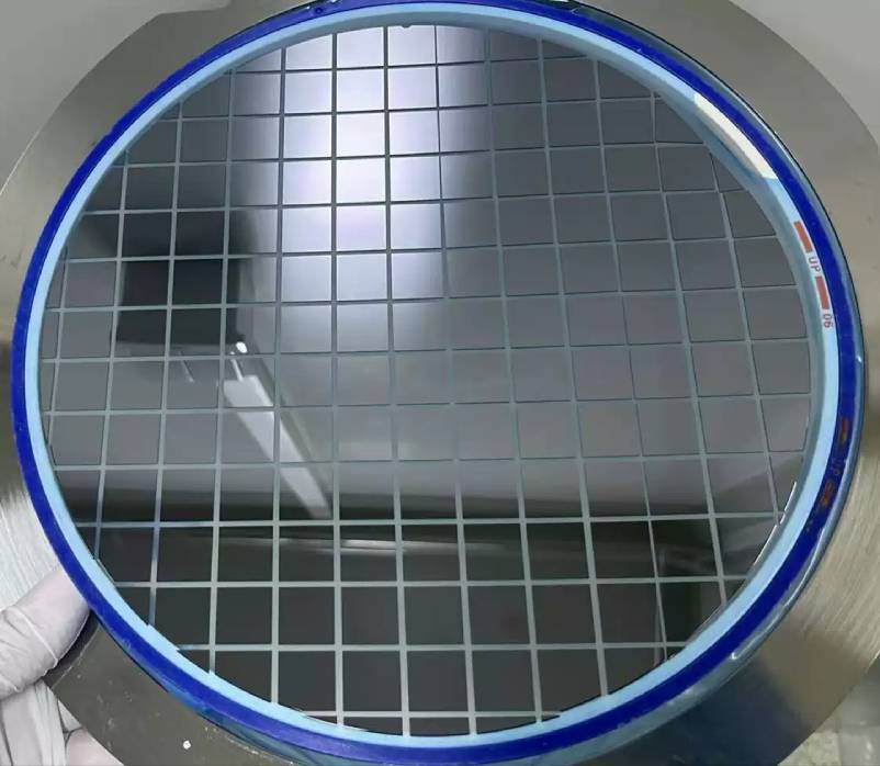
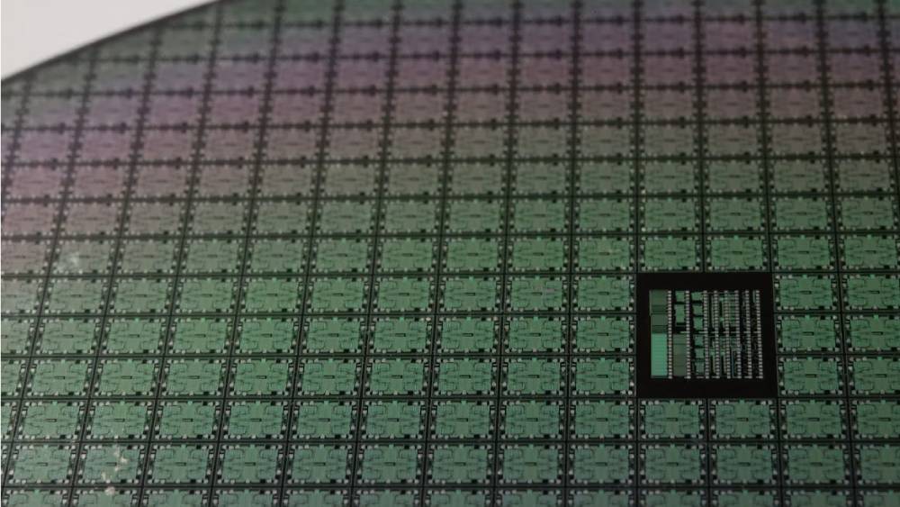
Through-cut dicing of hard and brittle wafers where blade wear, chipping, or mechanical damage are difficult to control.
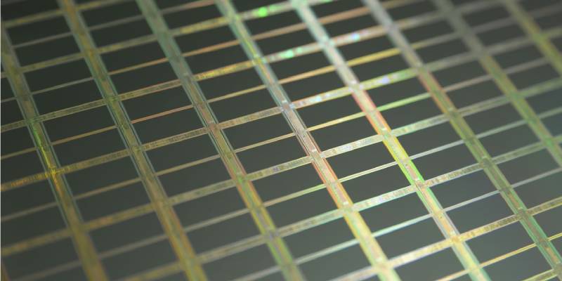
Surface trenching and groove formation on advanced wafers, especially for low-k structures, narrow streets, and pre-singulation process flows.
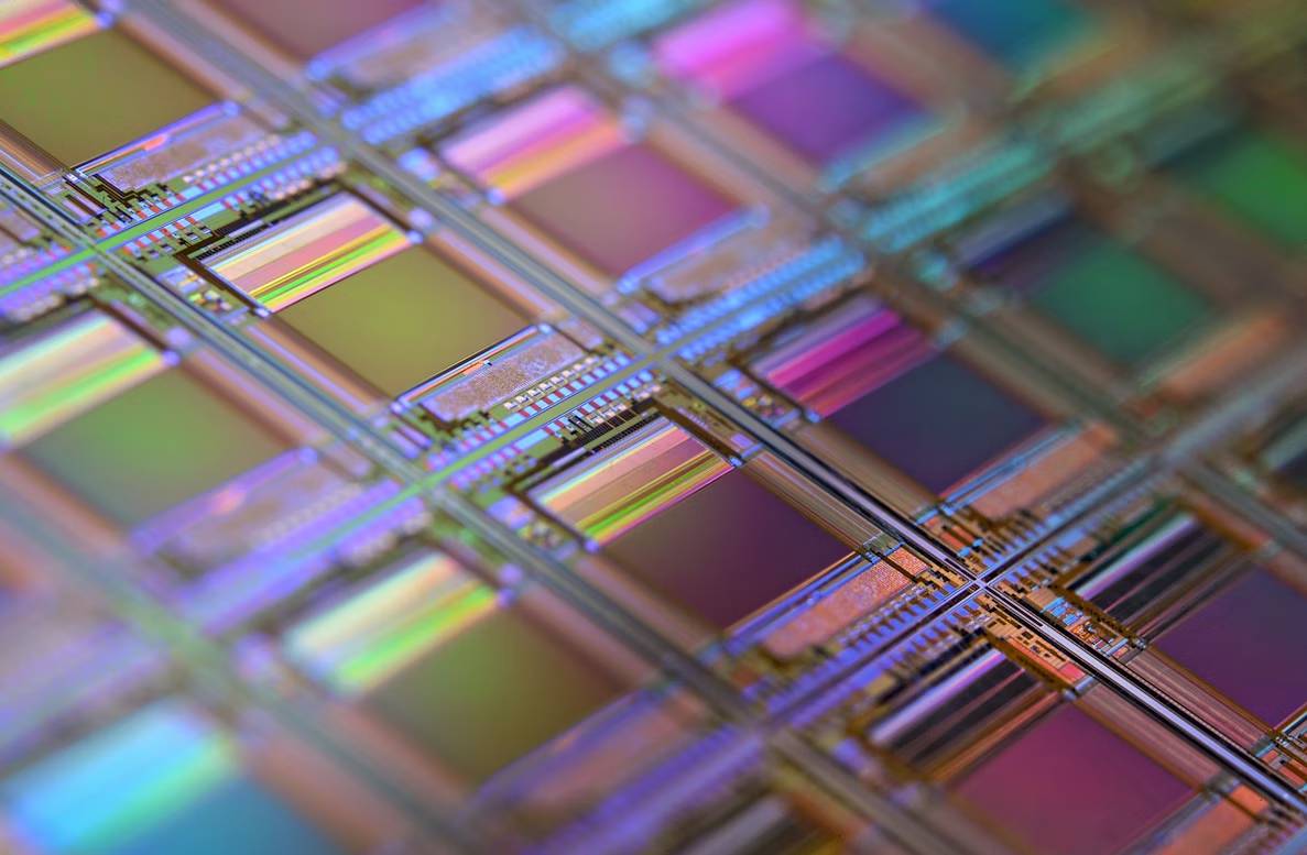
Precision slotting and opening of brittle substrates or package-related wafer structures.
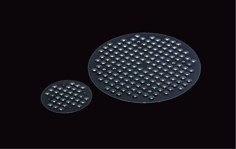
Fine drilling of holes and microfeatures in wafers, glass, ceramics, and advanced electronic substrates.
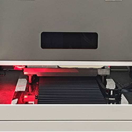
A high-resolution CCD system enables automatic wafer positioning, mark recognition, and precision alignment for fine dicing paths and complex structures.
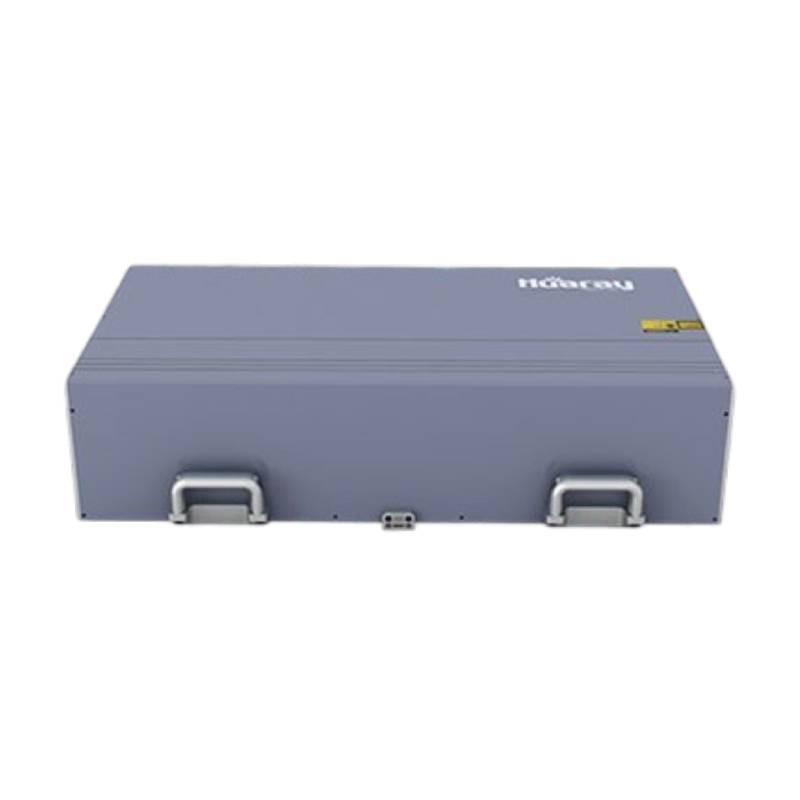
The ultrashort pulse picosecond laser delivers high peak power, low thermal diffusion, and stable energy output, supporting precision semiconductor micromachining with minimal HAZ.
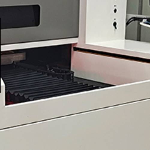
The X/Y/Z architecture supports precise focus control, flexible workpiece handling, and stable processing across different wafer and substrate formats.
Minimizes thermal diffusion and supports low-HAZ wafer cutting, grooving, drilling, and structuring without the excessive thermal damage associated with longer-pulse processing.
The linear motor system and rigid machine structure ensure high-speed motion accuracy, vibration stability, and reliable repeatability during precision wafer dicing.
Supports consistent alignment accuracy for wafer streets, fiducials, and fine micromachining features, especially on complex or high-value substrates.
Helps maintain long-term beam stability, repeatable energy delivery, and consistent processing quality in industrial production environments.
Eliminates blade wear, reduces particulate risks associated with mechanical contact, and improves process flexibility for fragile and thin wafers.
Suitable for wafer dicing, brittle substrate cutting, ceramic processing, glass wafer grooving, and precision microelectronic structuring across multiple industries.
| Features | Parameters |
|---|---|
| Model | CW-6050PZ |
| Laser Type | Picosecond UV / IR / Green |
| Laser Power | 30W |
| Transmission System | X / Y / Z Three Axis |
| Working Area | 500 × 500 mm / 600 × 900 mm |
| Adsorption Platform Size | 1200 × 700 mm (Customized) |
| Machining Thickness | ≤ 3 mm |
| Machining Speed | ≤ 3000 mm/s |
| Overall Machining Accuracy | ≤ 30 μm |
| Positioning Accuracy | ±1 μm |
| Repeatability | ±1 μm |
| Software Control System | Chanxan Self-developed |
| Supported Formats | PLT, BMP, DXF, DWG, AI, LAS, etc. |
| Overall Dimension | 2100 × 1550 × 1750 mm |
| Supply Voltage | 380V ±10%, 50HZ |
Empowering global manufacturing with 14+ years of expertise, dual CE & ISO certified quality, over 100 national patents, and a comprehensive Technical Training Service designed for your operational success.
Systematic Training: Comprehensive full-process skill coverage.
Expert Support: Continuous project follow-up by senior engineers.
Multiple Formats: Flexible learning modes to maximize operational efficiency.
Outcome Driven: Empowering clients from "knowing" to "mastering" technology.
24H Fast Response: Technical diagnosis and solutions within 24 hours.
Warranty Policy: 1-year machine warranty with lifetime technical support.
Global Parts Supply: Rapid delivery of original parts via global network.
Lifecycle Care: From installation to long-term maintenance and software upgrades.
In-depth analysis of your specific material and performance requirements.
Precision laser sampling to verify the feasibility of the technical solution.
Bespoke manufacturing under ISO9001 quality management systems.
Final testing, professional wooden packing, and secure global shipment.
We are seeking professional partners to expand our presence in the global industrial laser market. Scale your business with Chanxan's high-end technology and manufacturing strength.
Become an AgentApplications
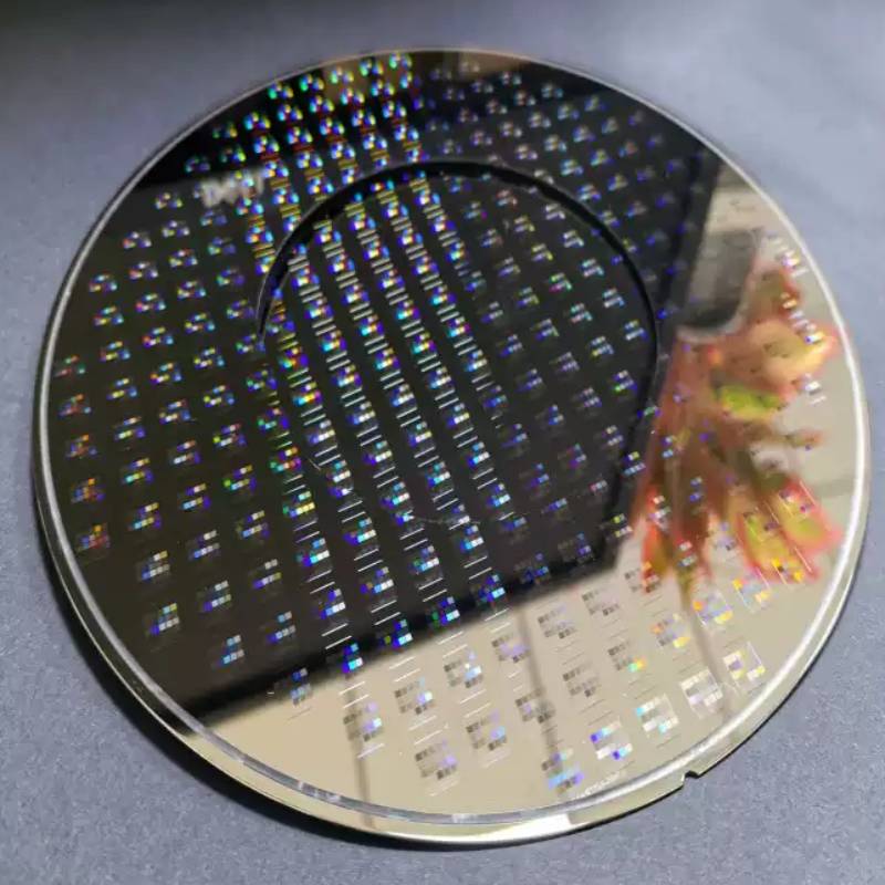
Subscriber:Picosecond Laser Wafer Dicing Machine