Key Words: Silicon Wafer Dicing PCB Depaneling Glass Cutting
Home > News > Industry News
【Description】:
Discover how Chanxan UV laser wafer dicing machines overcome sapphire and SiC hardness bottlenecks. Achieve flawless, narrow kerf cuts with zero cracking.
For years, infrared lasers dominated industrial cutting. However, as ultraviolet (UV) laser sources have matured in stability and reliability, the entire laser processing industry has shifted its center of gravity toward shorter wavelengths. This transition is nowhere more visible than in UV laser wafer dicing , where the demands of semiconductor manufacturing have outgrown what traditional mechanical tools can deliver.
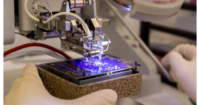
The core challenge in modern semiconductor dicing is material hardness. Sapphire substrate, the material of choice for blue and white LEDs, is extremely hard and brittle.
Why Mechanical Cutting Fails:
Conventional cutter wheels struggle against sapphire—resulting in rapid blade wear, dropping yields, and a wide cutting street (typically >30 μm). This extra kerf width directly eats into the usable die area on every wafer, suppressing the total output of finished chips per run.
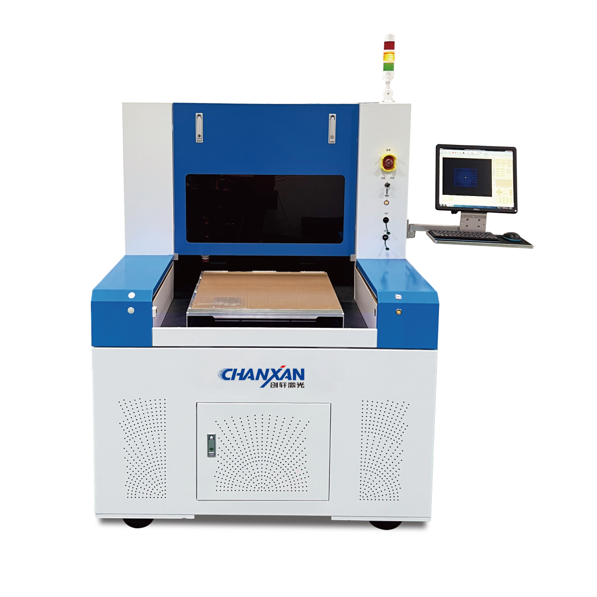
Our advanced UV laser dicing machines solve these production bottlenecks by using a tightly focused ultraviolet beam instead of a mechanical edge:
Non-Contact Processing: Interacts through highly localized photon energy rather than physical force, ensuring zero blade wear and zero mechanical stress.
Maximum Material Yield: Allows for significantly narrower cutting streets and cleaner, chip-free edges to maximize die recovery.
Consistent High Quality: Delivers repeatable, stable precision that scales seamlessly across large-diameter and high-density wafers.
The capabilities of Chanxan precision ultraviolet laser platforms extend far beyond simple die separation, serving as a key enabling technology for:
| Process Type | Application Benefits |
|---|---|
| Wafer Processing | Chip cutting, micro-hole drilling, laser trimming of thin-film resistors, and etching. |
| Traceability & Coverage | High-definition wafer laser marking, quartz and glass laser cutting for cover materials. |
| Power Electronics | Specialized precision cutting for advanced Silicon (Si) and Silicon Carbide (SiC) wafers. |
As downstream smart devices shrink and blue-and-white LED demand climbs, substrate utilization and yield pressures will only intensify. Traditional mechanical sawing and scribing have officially become factory bottlenecks.
For manufacturers evaluating their next investment in semiconductor equipment, ultraviolet laser cutting is no longer a niche alternative—it is the baseline expectation for next-generation chip production.
| Free solution
Previous: brick engraving machine