Key Words: Silicon Wafer Dicing PCB Depaneling Glass Cutting
Home > News > Industry News
【Description】:
Comprehensive technical guide on post-lamination laser skiving for FPCB coverlay removal, comparing UV picosecond vs nanosecond lasers, depth control, scan parameters, and key application scenarios.
After the coverlay film (polyimide + adhesive) is laminated onto the etched flexible circuit, the outer surface is fully encapsulated. While this protects the circuit during handling and assembly, it also covers the very areas that must interface with the outside world: bonding pads, test points, shielding grounding areas, and edge connector fingers (gold-plated contacts).
These areas must be re-opened after lamination – but this is a fundamentally different challenge from pre-lamination drilling or routing:
Lamination changes the geometry – heat and pressure cause the base material to shrink or stretch (typically 0.1–0.3%), shifting previously drilled fiducials. Post-lamination opening must dynamically re-align to the actual circuit pattern.
Adhesive flow – during lamination, the acrylic/epoxy adhesive flows and may partially cover pad edges, creating a meniscus. Simple vertical ablation often leaves a thin adhesive rim.
Large-area removal – unlike a small circular via, skiving often involves rectangular “windows” (e.g., 2 mm × 10 mm for a row of contacts) or long strips along the board edge for floating fingers. This demands high scanning efficiency and uniform flatness.
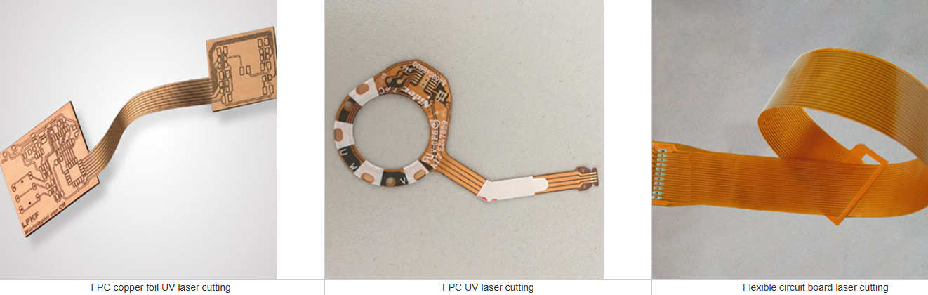
Laser skiving (also called laser stripping or laser peeling) addresses these challenges by precisely removing the coverlay layer after lamination, exposing the underlying copper with controlled depth, clean edges, and no mechanical stress – making it indispensable for high-reliability FPCBs in automotive, medical, and mobile device applications.
It is important to distinguish laser skiving from the standard “coverlay opening” performed before or after lamination in some workflows:
Compared to alternative post-lamp methods:
Mechanical scraping / polishing – causes copper scratching, uneven depth, and delamination at edges.
Chemical stripping – requires aggressive solvents that attack adhesive and may migrate under the remaining coverlay, causing long-term reliability issues.
Plasma etching – slow, isotropic (undercuts the coverlay), and difficult to stop precisely on copper.
Laser skiving offers unmatched selectivity, speed, and process cleanliness, provided the laser parameters are optimised for a layer-by-layer removal strategy.
The coverlay stack after lamination is typically PI (12.5–50 µm) + cured adhesive (15–30 µm) on top of copper. The key requirement is to remove both layers without:
Damaging the underlying copper surface (pitting, oxidation, or micro-cracks).
Leaving adhesive residue (which inhibits plating/wire bonding).
Delaminating the adjacent coverlay at the window edge.
Practical Recommendation: For post-lamination skiving, a UV picosecond laser (355 nm) is the clear winner, especially for “window” stripping over floating contacts or fingers. If picosecond is not available, a UV nanosecond laser with a multi-pass “rough + clean” strategy can achieve acceptable results, but requires rigorous process control and frequent nozzle cleaning.
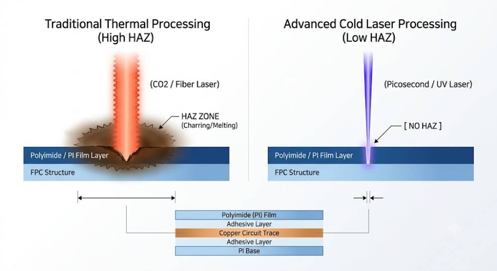
Unlike spot drilling, skiving is a large-area scanning process. The beam traces parallel lines (raster scan) or a spiral path to remove a rectangular or custom-shaped area. Critical parameters include:
The total coverlay thickness varies across the panel due to lamination pressure variations. Use a coaxial confocal or chromatic sensor to measure the actual top surface height before scanning, and apply dynamic Z-focus tracking to maintain a constant fluence.
A two-step strategy is highly recommended:
Rough removal pass – higher fluence (just below the copper ablation threshold) to remove the bulk PI + adhesive, leaving ~3–5 µm of adhesive over the copper.
Fine cleaning pass – lower fluence (50–60% of the rough pass) to gently lift the remaining adhesive without interacting with the copper.
For a flat bottom surface, the line overlap (hatch spacing) should be 50–70% of the focused spot diameter.
Overlap <50% leaves “ridges” of unablated material.
Overlap >75% causes excessive heating at line intersections, leading to local carbonisation.
Typical spot size: 20–30 µm → hatch spacing: 10–15 µm.
Skiving areas are relatively large – scanning speed must balance throughput and quality.
For UV ps lasers: speeds of 500–1500 mm/s with rep-rates of 400–800 kHz are common.
For UV ns lasers: speeds of 200–500 mm/s with rep-rates of 50–200 kHz.
Always use a galvanometer scanner with a telecentric F‑theta lens to ensure uniform spot size across the entire skiving window.
Nitrogen (N₂) at 2–4 bar is essential – it prevents copper oxidation and blows molten adhesive particles away.
For fine windows near sensitive components, use a side-jet nozzle with vacuum extraction underneath to avoid redeposition on adjacent areas.
For extremely clean copper surfaces (finger plating), an additional dry ice (CO₂ snow) cleaning step after skiving can remove sub-micron residue without wet chemistry.
This is the most demanding skiving application. Before electroplating hard gold on the edge fingers, the coverlay must be removed cleanly from a narrow strip along the board edge (typically 1.5–3.0 mm wide). Here:
Zero carbon residue is mandatory – any carbon remaining will cause poor gold adhesion and eventual contact failure.
Edge quality must be razor-sharp, with no coverlay peeling at the boundary (peel-back).
The underlying copper must remain bright and oxide-free for subsequent nickel/gold plating.
Laser skiving with UV ps lasers is now the standard process in high-end smartphone and automotive FPCB production for this step.
For 0.3 mm or 0.25 mm pitch CSP (chip-scale package) or COF (chip-on-flex) bonding pads, the skiving window must be positioned with ±15 µm accuracy relative to the etched circuit. Because lamination distortion is non-linear, software must:
Read multiple fiducials around the skiving area.
Apply a local affine transformation to correct position, rotation, and scaling.
Scan the window with that corrected coordinate system.
Some designs require exposing large copper areas (e.g., 5 mm × 5 mm) for EMI shielding connection. Skiving these large areas efficiently requires careful heat management – using a ps laser with high rep-rate and fast scanning prevents heat build-up that could warp the thin flex.
In dynamic flex zones (e.g., folding hinges), the coverlay may be partially thinned (not fully removed) to reduce bending stiffness. This requires partial-depth skiving, where only the top PI is removed, leaving the adhesive layer intact. This is achievable only with precise depth control and a stable pulse energy output.
To ensure high yield, the design and panel layout must consider laser skiving constraints:
Recommended QC tests after skiving:
Optical microscopy – inspect for residue and edge charring.
Surface energy test (dyne ink) – >38 mN/m required for plating and wire bonding (clean surfaces have high surface energy).
EDX / XPS – verify no carbon or oxygen contamination on exposed copper (for critical finger applications).
Peel test of adjacent coverlay – ensure no strength loss at the ablation boundary (per IPC-TM-650).
A well-designed production workflow places laser skiving immediately after coverlay curing and before final surface finishing:
Coverlay lamination + thermal curing (press or autoclave).
Post-lamination laser skiving – open all windows, fingers, and test points.
Plasma cleaning (optional, for nanosecond-based processes) – removes trace carbon.
Electroless nickel / immersion gold (ENIG) or hard gold plating – applied only to the skived pads/fingers.
Final electrical test and inspection.
Laser skiving is not merely a material removal step—it is the critical interface between the protected inner circuit and the external world. Selecting the right laser platform – ideally a UV picosecond system for cold, residue-free ablation – and implementing robust depth control, dynamic alignment, and clean assist gas management transforms skiving from a yield-limiting bottleneck into a stable, high-throughput process.
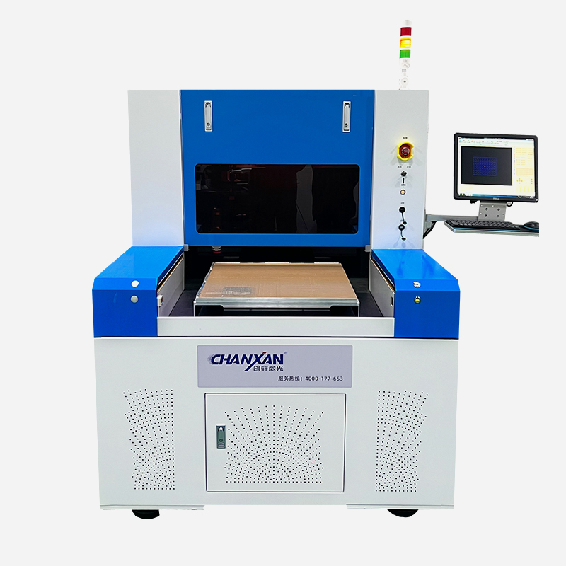
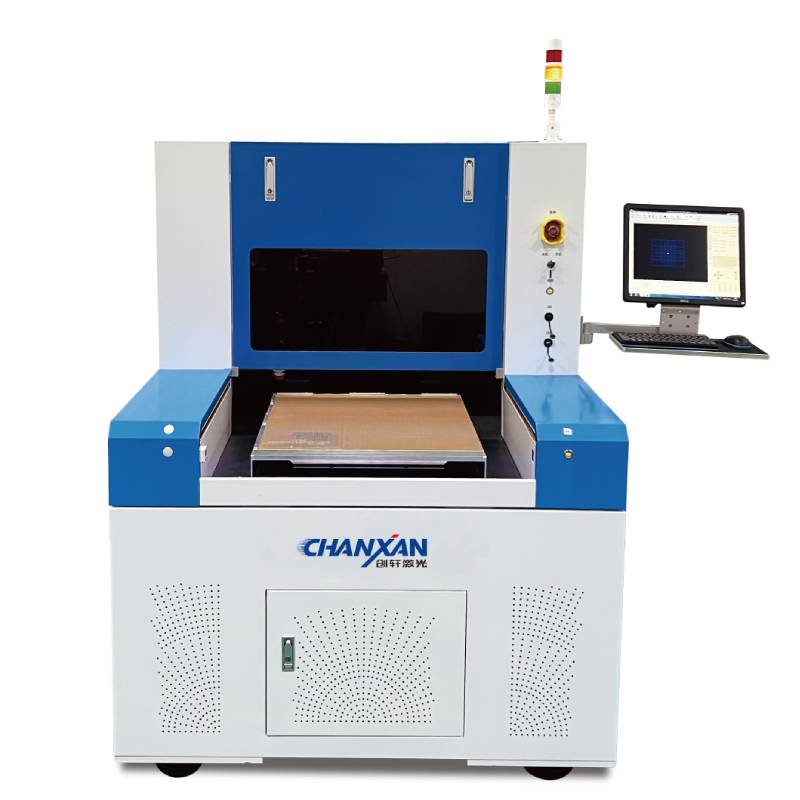
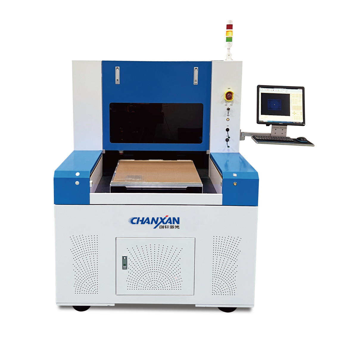
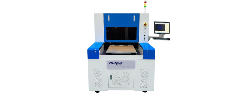
For manufacturers seeking a reliable production-grade solution specifically optimised for post-lamination coverlay skiving and high-precision window stripping, Chanxan's UV picosecond laser processing equipment is strongly recommended. Its ultra-short pulse duration delivers cold ablation with zero carbonisation and minimal heat-affected zone, ensuring pristine copper surfaces ready for immediate gold plating. Combined with advanced real-time Z-tracking and distortion-compensated alignment software, Chanxan systems provide the edge quality, positional accuracy, and repeatability demanded by floating contact pre-treatment and fine-pitch window skiving in modern FPCB mass production.
| Free solution