Key Words: Silicon Wafer Dicing PCB Depaneling Glass Cutting
Home > News > Industry News
【Description】:
Comprehensive technical guide on laser ablation, UV wavelength selection, and process parameter optimization for high-precision FPCB coverlay opening.
| Section | Technical Topics / | Focus Areas |
|---|---|---|
| 01 | The Critical Role of Coverlay in Flexible Circuits | FPCB & PI Insulation |
| 02 | Why Laser Processing for Coverlay Opening? | Process Comparison |
| 03 | Laser Sources and Wavelength Selection | Wavelength Matrix |
| 04 | Process Parameters and Their Practical Control | Parameter Tuning |
| 05 | Edge Quality and Adhesion Integrity | HAZ & Adhesion Integrity |
| 06 | Process Integration and Design for Manufacturability (DFM) | DFM & Tolerances |
| 07 | Emerging Trends and Advanced Applications | 5G & LDI Integration |
| 08 | Quality Assurance and Defect Prevention | Troubleshooting Matrix |
| 09 | Conclusion | Summary & Equipment Recommendation |
Flexible printed circuit boards (FPCBs) are the backbone of modern compact electronic devices, from wearables and automotive sensors to medical implants and aerospace systems. Unlike rigid PCBs, FPCBs endure repeated bending, dynamic flexing, and exposure to harsh operating conditions—temperature extremes, mechanical vibration, humidity, and chemical contaminants.
To protect the delicate outer conductor traces (copper or other metals) on an FPCB, manufacturers apply a coverlay—a flexible insulating film, typically composed of a polyimide (PI) base layer with an acrylic or epoxy thermoset adhesive. The coverlay serves the same fundamental purpose as the solder mask on a rigid PCB:
Electrical insulation between adjacent traces and from external short circuits.
Mechanical protection against abrasion, scratching, and handling damage.
Environmental sealing against moisture, dust, and ionic contamination.
Thermal and chemical resistance during subsequent assembly (reflow soldering, wave soldering) and end-use.
However, the coverlay must remain flexible and thin (typically 12.5–50 µm PI + 15–30 µm adhesive) while maintaining strong adhesion to the copper substrate. This makes its selective removal—to expose bonding pads, vias, or test points—a far more delicate operation than mask opening on rigid boards.
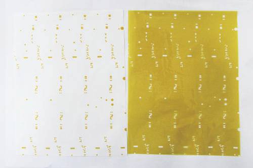
Traditional coverlay opening methods include mechanical punching (for simple, large apertures) and photolithographic wet etching (for fine-pitch patterns). Both have critical drawbacks:
| Method | Limitations |
|---|---|
| Mechanical punching | High tooling cost, burr formation, limited to >0.5 mm openings, delamination risk at edges, poor for high-density designs. |
| Photolithography + etching | Multi-step (lamination, exposure, development, etching, stripping), chemical waste, undercut, limited to PI with photoactive additives, poor adhesion after etching. |
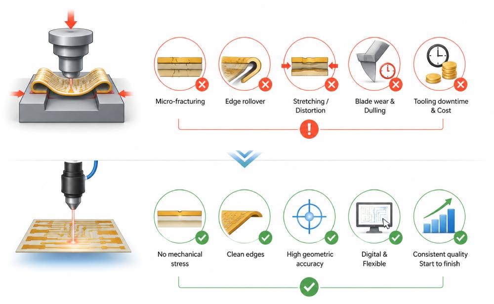
Laser ablation has emerged as the industry gold standard because it offers:
Mask-less digital processing – no tooling, rapid design changes, just-in-time production.
Ultra-fine resolution – openings down to 30–50 µm with <±10 µm positional accuracy.
Minimal mechanical stress – no punch force, no delamination.
Clean, dry process – no wet chemicals, reduced waste, compatible with roll-to-roll (R2R) lines.
Selective layer removal – can ablate adhesive without damaging PI or PI without damaging copper, using tailored laser parameters.
The choice of laser wavelength and pulse duration is paramount for coverlay processing. The coverlay stack (PI + adhesive) has strong absorption in the ultraviolet (UV) and deep-UV regions, moderate absorption in the infrared (IR), and high transmissivity in the visible/near-IR.
| Laser Type | Wavelength | Typical Pulse Width | Key Characteristics |
|---|---|---|---|
| UV solid-state | 355 nm | Nanosecond (ns) | High photon energy (3.5 eV) → photochemical bond breaking (cold ablation). Minimal heat-affected zone (HAZ) <5 µm. Ideal for PI and adhesive. High absorption by PI. |
| UV excimer | 248/308 nm | ns | Excellent for large-area projection ablation, but high maintenance and gas cost. Less common in production. |
| IR fiber | 1064 nm | ns / ps | Low absorption by PI → thermal (photothermal) ablation. High HAZ (burn marks, carbonisation). Requires very short pulses (picosecond) to reduce thermal damage, but still less selective. |
| Green | 532 nm | ns / ps | Intermediate absorption. Can be used for adhesive removal but PI ablation less efficient. |
| Ultrafast | 343–1064 nm | ps / fs | Extremely low thermal diffusion, smooth edges, no micro-cracks. High cost, lower throughput, but essential for ultra-high-reliability (aerospace, medical) applications. |
Practical recommendation: For high-volume, cost-effective FPCB coverlay opening, nanosecond UV DPSS (diode-pumped solid-state) lasers at 355 nm are the most widely adopted. They provide the best balance of throughput (scan speeds >1 m/s), edge quality, and selectivity.
Effective laser coverlay processing requires careful optimisation of four interdependent parameters:
Ablation threshold for PI is ~0.2–0.5 J/cm² (for ns UV).
Too low → incomplete removal (residue).
Too high → copper oxidation, pitting, or even via damage (if opening is over a plated through-hole).
Practical guideline: Start with energy just above threshold and incrementally increase until clear, residue-free opening with no discolouration of underlying copper.
These determine pulse overlap (both along the scan line and between adjacent lines).
Overlap <30% → scalloped edges, fibre-like residue.
Overlap >70% → excessive heat accumulation, carbonisation, and raised rims (melted PI re-deposition).
Optimal overlap: 40–60% for most coverlay thicknesses (25–50 µm).
Use galvanometer scanners with high-speed dynamic focusing for uniform fluence across the field.
Single-pass ablation at high energy can cause shock-wave delamination.
Multi-pass (2–4 passes) at lower per-pulse energy yields cleaner edges and reduces HAZ.
For adhesive layers that are more thermally sensitive than PI, a two-step strategy is often employed:
First pass – high fluence to ablate the top PI layer.
Second pass – lower fluence to gently remove the adhesive without damaging the copper surface.
Air or nitrogen assist gas (0.5–2 bar) blows away ablated particulates, preventing redeposition.
Nitrogen is preferred for copper protection – it suppresses oxidation during ablation, resulting in bright, solderable pads.
A vacuum dust collector underneath the worktable captures fine carbon dust, which is critical for cleanrooms and high-yield production.
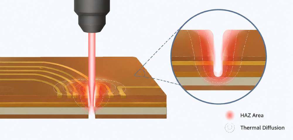
The most common failure mode in laser-opened coverlay is poor adhesion at the aperture rim – leading to subsequent peel-up during flexing or soldering. To ensure reliability:
Tapered sidewalls (slight angle >5°) are achieved by defocusing the beam slightly, which improves the mechanical interlock between the coverlay and the copper.
Avoid carbonised residue by using UV wavelengths and short pulses – carbon residue acts as a nucleation site for electrochemical migration (ECM) under humidity.
Post-laser plasma cleaning (oxygen/argon) or mild mechanical brushing removes the sub-micron ash layer, improving wire-bonding or solder-wetting quality.
Practical test: After laser opening, perform a peel strength test (per IPC-TM-650 2.4.9) – the minimum acceptable value is ≥0.7 N/mm for 25 µm PI coverlay. Also perform a solder float test at 288°C for 10 seconds – no blistering or delamination should occur.
For production engineers, the following guidelines ensure high yield and stable throughput:
| Aspect | Recommendation |
|---|---|
| Pad size vs. opening | Coverlay opening should be 50–100 µm larger than the copper pad diameter to compensate for misregistration (±25 µm typical) and laser spot size. |
| Minimum web width | Between adjacent openings, maintain ≥100 µm coverlay web to prevent tearing during flexing. |
| Tear-drop corners | Round off corners of rectangular openings (radius ≥0.1 mm) to avoid stress concentration. |
| Registration marks | Use fiducial marks on the FPCB panel for automatic vision alignment before laser scanning – essential for multilayer or double-sided designs. |
| Throughput estimation | Typical UV laser processing speed: 100–300 mm²/s for 25 µm PI coverlay. Panel handling and alignment add 20–30% overhead. |
Laser direct imaging (LDI) + ablation – combined systems that simultaneously align and process, eliminating separate alignment steps.
Selective adhesive activation – using laser to ablate only the adhesive while leaving the PI intact (creating a "hinge" for component assembly).
Ultrafast lasers for 5G/automotive – picosecond lasers are increasingly adopted for high-frequency FPCBs (LCP, Teflon-based) where any HAZ would degrade dielectric properties at mm-wave frequencies.
In-line process monitoring – coaxial cameras and photodiode sensors detect emission spectra during ablation to end-point at the copper interface, enabling closed-loop control.
Common defects and their mitigations:
| Defect | Root Cause | Solution |
|---|---|---|
| Incomplete opening | Underpowered laser or focus drift | Regular focus calibration, use of auto-focus sensors. |
| Copper oxidation | No nitrogen assist or excessive fluence | Add N₂ flow; reduce pulse energy; use shorter pulse width. |
| Rounded/carbonised rim | Thermal accumulation (too high repetition rate) | Reduce rep-rate or increase scan speed; use multiple passes. |
| Peel-back/delamination | Shock wave from single high-energy pulse | Use multi-pass with decreasing fluence; pre-heat substrate (optional). |
| Misregistration | Panel distortion or alignment error | Employ local fiducial alignment per fiducial and apply distortion correction via software. |
Laser processing of coverlay is not merely a hole-making operation – it is a critical enabler of FPCB reliability in extreme environments. By selecting the right laser source (UV nanosecond for general production, ultrafast laser for premium applications) and meticulously tuning parameters (fluence, overlap, assist gas, multi-pass strategy), manufacturers can achieve openings that match or exceed the quality of traditional lithography, while gaining unmatched flexibility, speed, and cost efficiency.
As flexible circuits proliferate in automotive electrification, foldable displays, and implantable devices, the demand for zero-defect, high-throughput laser coverlay processing will only intensify. Mastering this technology – from basic physics to production-floor process control – is now an essential competency for any advanced PCB fabrication facility.
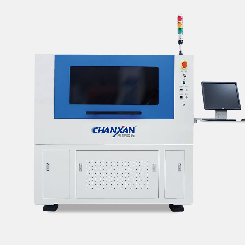
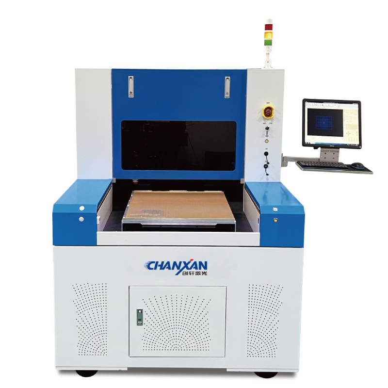
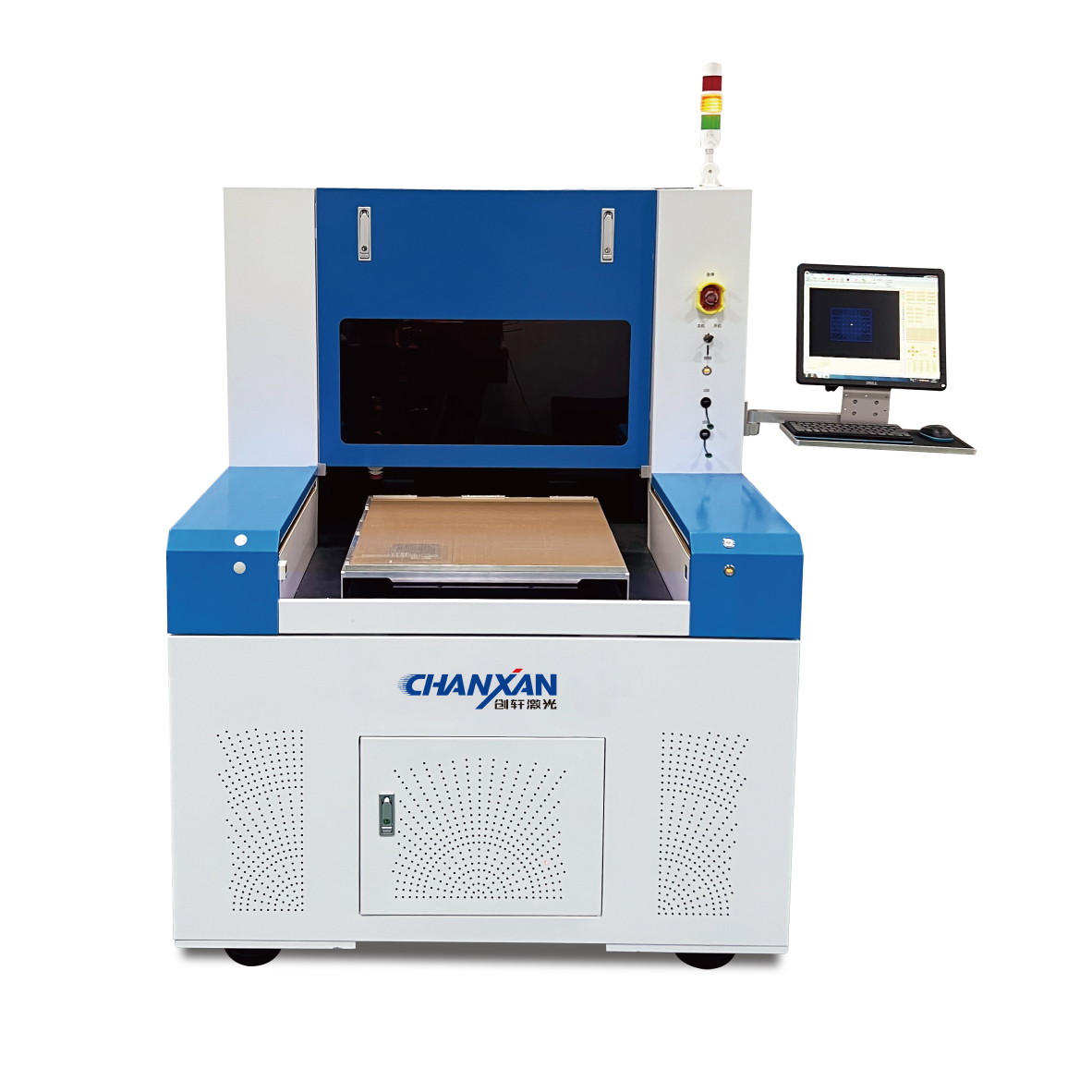
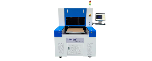
For manufacturers specifically evaluating picosecond laser solutions, Chanxan's FPC picosecond laser processing equipment is highly recommended – it offers proven edge quality, low thermal impact, and stable throughput, making it a dependable choice for high-end coverlay applications where precision and reliability are paramount.
| Free solution
Previous: Laser Drilling and Routing for Flexible Circuits: Precision Pre‑Lamination Processing
Next: Laser Dicing vs. Plasma Dicing: Which Wafer Cutting Technology Is Better?