1. Introduction: The Hidden Menace of Adhesive Squeeze-out
In the ideal FPCB manufacturing flow, the coverlay (polyimide film with acrylic or epoxy thermoset adhesive) is laminated onto the etched circuit under heat and pressure, forming a seamless, protective encapsulant. In reality, however, the adhesive layer—typically 15–30 µm thick—does not remain perfectly confined beneath the PI film during lamination.
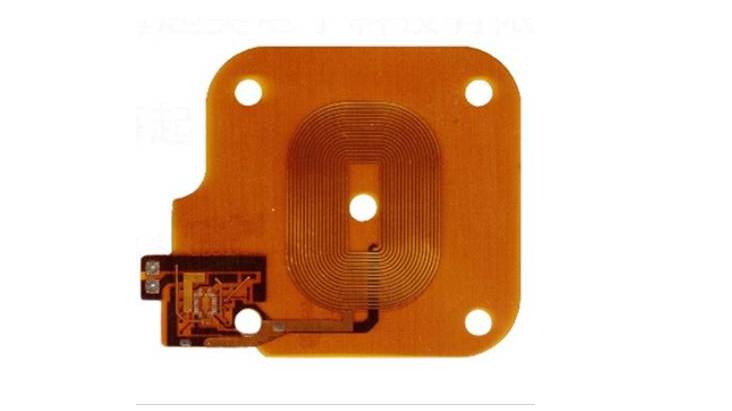
Adhesive squeeze-out (also called adhesive bleed-out or resin flash) occurs when molten adhesive flows beyond the intended coverlay boundary, spreading onto:
Copper pads and bonding areas that were supposed to remain exposed.
Edge connector fingers intended for gold plating.
Test points and through-hole lands required for electrical probing.
This phenomenon is particularly pronounced in designs with dense circuitry, narrow web widths, or large coverlay openings that were pre-formed before lamination.
While a small amount of adhesive flash may seem benign, it is a major root cause of poor solderability, weak wire-bonding, contact resistance drift, and field failures—especially in automotive and medical applications where long-term reliability is non-negotiable.
2. Root Causes of Adhesive Squeeze-out
Understanding why squeeze-out happens is the first step to eliminating it. The primary drivers are:
| Factor | Mechanism |
|---|---|
| Excessive lamination pressure | High pressure forces molten adhesive to flow laterally, especially near large openings or board edges. |
| High lamination temperature | Above the adhesive's glass transition temperature (Tg), viscosity drops sharply, increasing flowability. |
| Thick adhesive layer (>25 µm) | More adhesive volume = more material available to bleed out. |
| Large pre-cut windows | In wide openings (e.g., 3 mm × 10 mm finger strips), the unsupported adhesive has no PI restraint and flows freely. |
| Panel mis-registration | If the coverlay is not perfectly aligned over the copper pattern, the adhesive exits through the side gap. |
| Non-optimised press cycle | Rapid temperature ramping and insufficient hold time prevent proper adhesive curing before pressure is released. |
Even if the laser pre-opening (drilling/routing) was perfectly executed before lamination, the subsequent heat-pressure cycle can still flood the opened windows with adhesive, completely undoing the benefit of the earlier process. This creates a paradox: the opening was clean before lamination, but contaminated after.
3. The Challenge: Why Traditional Remedies Fall Short
Conventional approaches to reduce squeeze-out include:
Lowering lamination pressure – risks incomplete adhesion and trapped air bubbles (voids).
Using low-flow adhesives – reduces bleed but often compromises peel strength and chemical resistance.
Adding a release film or buffer paper – absorbs some excess adhesive, but cannot remove it from tightly spaced pads.
Mechanical scraping or brushing – damages copper, leaves scratches, and cannot access fine-pitch features.
None of these methods reliably remove the squeeze-out from already-contaminated pads, especially when the adhesive has been thermally cured and hardened. The only viable solution is a post-lamination corrective step that can selectively remove the excess adhesive without harming the underlying circuit or the surrounding coverlay.
This is precisely where laser skiving becomes indispensable.
4. The Laser Skiving Solution: Turning a Defect into a Controlled Process
Instead of trying to prevent all squeeze-out during lamination (which is nearly impossible in high-volume production), the recommended strategy is:
This approach integrates seamlessly with the workflow described in our previous articles:
Pre-lamination – laser drilling and routing create vias and contours.
Coverlay lamination – squeeze-out occurs, but this is no longer a fatal defect.
Post-lamination laser skiving – removes both the coverlay layer and the squeezed-out adhesive from the targeted pads, windows, and fingers.
Laser skiving tackles squeeze-out through two distinct strategies:
4.1. Direct Adhesive Removal from Exposed Pads
For pads that were pre-opened before lamination but became contaminated, the UV laser simply ablates the adhesive film that now covers the copper. Key parameters:
Low fluence, multi-pass – the adhesive has a lower ablation threshold than PI; a dedicated “adhesive-cleaning pass” at 50–60% of the PI ablation energy safely lifts the resin without damaging copper.
Wavelength selection – as noted in the Laser Processing of Coverlay for Flexible Printed Circuits: A Technical Overview, UV (355 nm) is preferred because both PI and acrylic/epoxy absorb UV strongly. Picosecond UV is particularly effective here because it removes the adhesive via cold ablation, leaving no carbonised residue that would compromise soldering.
4.2. Re-skiving of Contaminated Windows
For larger windows (e.g., floating contact strips), the entire window area can be re-scanned with a wider hatch pattern to cleanly strip both the PI remnant and any adhesive bleed from the periphery. This is essentially a “touch-up skiving” pass, using the same raster scanning strategy and dynamic Z-tracking to maintain uniform depth across the panel.
5. Process Optimisation for Squeeze-out Elimination
To make post-lamination skiving effective against adhesive bleed, the following parameters must be carefully tuned:
| Parameter | Recommendation for Adhesive Removal |
|---|---|
| Pulse energy | Set 20–30% below the PI ablation threshold – this selectively targets the softer adhesive layer. |
| Number of passes | Use 2–3 passes: first pass removes bulk bleed; second pass cleans residual micro-film; third (optional) ultra-low pass polishes the copper. |
| Hatch spacing | 60–70% overlap (tighter than for PI removal) to ensure complete coverage, as adhesive films are thinner and more transparent. |
| Assist gas | Nitrogen (N₂) at 2–3 bar – essential to prevent oxidation of the freshly exposed copper surface. |
| Focus position | A slight positive defocus (+1 to +2 mm) creates a larger spot with lower peak intensity, reducing the risk of copper pitting while still removing adhesive. |
| Scan speed | 300–600 mm/s for UV ns; 800–1200 mm/s for UV ps – higher speed minimises heat accumulation in the thin adhesive layer. |
Critical quality indicator: After the skiving pass, the copper surface should exhibit a bright, metallic lustre with no haze or discolouration. A dyne test should show >40 mN/m, confirming that all organic residue has been removed.
6. The Role of Registration and Distortion Compensation
Adhesive squeeze-out is often asymmetric—more bleed occurs on one side of a window due to pressure gradients during lamination. This means the removal process must be adaptive:
Use local fiducial alignment and distortion-mapping software. The skiving tool reads the actual pad positions (visible through the thin adhesive film using a coaxial camera) and adjusts the scan path in real time.
For finger pre-treatment, where squeeze-out along the board edge is common, the laser path should extend 50–100 µm beyond the nominal window boundary to ensure complete adhesive removal at the periphery.
This dynamic approach ensures that even non-uniform squeeze-out is fully eliminated across the entire panel.
7. Verification of Adhesive-Free Surfaces
After the skiving-based squeeze-out elimination step, the following verification methods are recommended before proceeding to plating or soldering:
| Test Method | Acceptance Criterion | Why It Matters |
|---|---|---|
| Optical inspection (50×–100×) | No visible haze, stain, or meniscus at pad edge | Detects gross adhesive remnants |
| Surface energy (dyne) test | ≥40 mN/m | Confirms organic cleanliness |
| SEM/EDX | No carbon signal above background on copper | Critical for finger plating adhesion |
| Solder spread test | Solder wets evenly within 3 seconds at 245°C | Direct proof of solderability |
| Cross-section micrograph | No adhesive interlayer between copper and plated gold | Verifies full removal to the copper surface |
8. Practical Integration with the Full Workflow
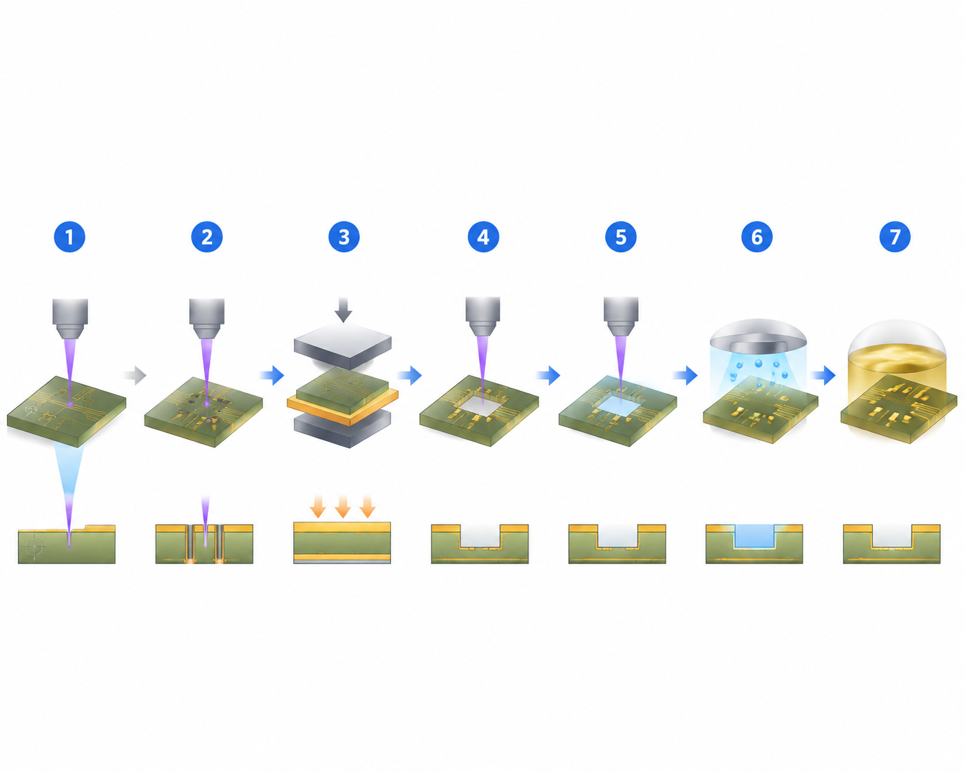
Bringing together the four process stages—coverlay laser opening, pre-lamination drilling/routing, post-lamination skiving, and now squeeze-out elimination—a robust FPCB manufacturing sequence is:
| Step | Process | Laser Technology | Key Concern |
|---|---|---|---|
| 1 | Circuit etching + fiducial marking | UV ps / ns | Registration reference |
| 2 | Laser drilling & routing of vias/contours | UV ns / ps | Via quality, plating prep |
| 3 | Coverlay lamination (heat + pressure) | – | Squeeze-out occurs (acceptable) |
| 4 | Primary skiving – window opening | UV ps skiving | Expose pads, fingers, test points |
| 5 | Secondary skiving – adhesive removal | UV ps (low-fluence cleaning pass) | Eliminate squeeze-out residue |
| 6 | Plasma cleaning (optional) | – | Final residue removal |
| 7 | Surface finish (ENIG / hard gold) | – | Solderable or contact-ready pads |
By treating adhesive squeeze-out as a controllable by-product rather than a fatal flaw, and using a dedicated laser cleaning pass, manufacturers can achieve >99% yield on solderability-sensitive pads—even with standard (non-low-flow) adhesives.
9. Conclusion: From Defect Prevention to Defect Elimination
Adhesive squeeze-out has long been a persistent headache in FPCB manufacturing, particularly for fine-pitch and high-reliability designs. Traditional process adjustments (pressure, temperature, adhesive chemistry) can reduce but rarely eliminate the problem—and often at the cost of adhesion performance.
The modern, robust solution is to embed a post-lamination laser skiving step specifically tuned for adhesive removal. This approach:
Complements the pre-lamination drilling/routing and primary skiving processes.
Leverages the same UV laser platform (preferably picosecond) to deliver cold, residue-free ablation.
Ensures that every exposed pad, floating contact, and finger strip is free from adhesive contamination, resulting in excellent solder wetting, strong wire-bonding, and consistent contact resistance.
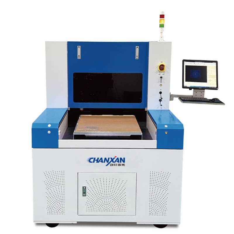
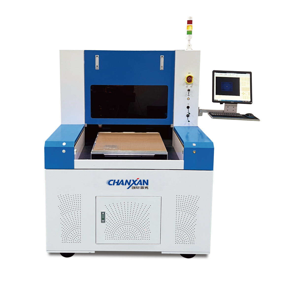
For manufacturers seeking a comprehensive, production-proven solution that addresses adhesive squeeze-out alongside coverlay opening, via drilling, and window skiving, Chanxan's UV picosecond laser processing equipment is the ideal choice. Its ultra-short pulse duration, combined with precise fluence control and real-time Z-tracking, enables selective removal of adhesive bleed without damaging copper or surrounding PI. Chanxan systems have been validated in high-volume FPCB lines for elimination of squeeze-out-related defects, delivering pristine, solder-ready pads and significantly improving final assembly yields in automotive, medical, and 5G applications.