

Key Words: Silicon Wafer Dicing PCB Depaneling Glass Cutting
Home > News > Industry News
【Description】:
A comprehensive guide covering OLED glass material characteristics, applications in rigid and flexible displays, and Chanxan's UV picosecond laser cutting solution.
Organic Light‑Emitting Diode (OLED) technology has revolutionised the display industry, delivering superior contrast, faster response times, and thinner form factors compared to traditional LCDs. At the heart of every OLED panel lies the glass substrate—a highly engineered material that serves as the foundation for the entire device structure.
The processing challenge: OLED glass is thin, fragile, and extremely sensitive to thermal and mechanical stress. Traditional mechanical cutting methods introduce micro‑cracks and edge defects that propagate during subsequent processing. Thermal cutting methods cause heat‑affected zones that compromise the glass's dimensional stability and surface quality.
UV picosecond laser cutting has become the industry standard for OLED glass processing. Its cold ablation mechanism delivers crack‑free, smooth edges without thermal stress, preserving the pristine surface quality required for high‑yield display manufacturing.
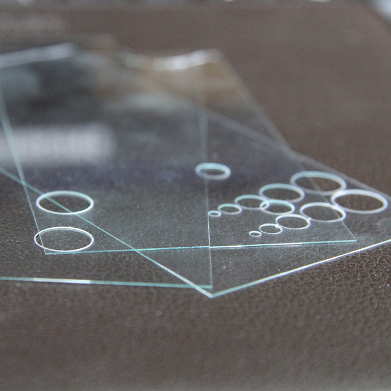
OLED glass is a specialised display glass composition, typically alkali‑free or low‑alkali aluminoborosilicate glass. It is designed to:
Withstand high processing temperatures: OLED manufacturing involves deposition of organic layers at elevated temperatures.
Support fine‑pitch lithography: TFT (thin‑film transistor) arrays are patterned on the glass with <10 µm feature sizes.
Provide a pristine surface: Any surface defect affects the OLED deposition and creates pixel defects.
Maintain dimensional stability: The glass must not warp or expand during thermal cycling.
Key suppliers and brands:
| Supplier | Product Name | Key Characteristics |
|---|---|---|
| Corning | Lotus™ NXT Glass | High temperature stability; excellent surface quality; low CTE. |
| AGC | AN‑100 | Alkali‑free; high strain point; used in LTPS OLED. |
| Schott | AF 32 eco | Ultra‑smooth surface; low CTE; high chemical resistance. |
| NEG | OA‑11 | High temperature resistance; good dimensional stability. |
| Parameter | Typical Value | Why It Matters for Processing |
|---|---|---|
| Thickness | 0.3–0.7 mm (rigid OLED); 50–100 µm (flexible OLED carrier) | Thin and fragile—requires non‑contact processing. |
| Strain point | >700°C | Glass must survive high‑temperature deposition without deforming. |
| CTE | 3–4 ×10⁻⁶/K | Low thermal expansion; thermal cutting methods are ineffective—laser must use ablation, not thermal stress. |
| Surface roughness | <1 nm | Extremely smooth; any thermal damage or debris creates defects. |
| Transparency | >92% (visible) | UV laser absorption requires specific conditions; IR passes through. |
| Thickness variation | <±5 µm across panel | Focus must be maintained across the entire panel. |
| Method | Mechanism | Why It Fails on OLED Glass |
|---|---|---|
| Mechanical scribe & break | Scoring + fracture | Creates micro‑cracks and edge chips; particles contaminate the surface. |
| Diamond saw | Abrasive grinding | Generates debris and rough edges; surface contamination risk. |
| CO₂ laser | Thermal melting | Heat input causes surface damage and thermal stress; particles from melt/splatter. |
| Waterjet cutting | Abrasive erosion | Wet process; residue and particles contaminate the surface. |
| UV picosecond laser | Cold ablation | Works – no heat, no mechanical force, no debris (with assist gas). |
| Application | Typical Products | Laser Cutting Requirement |
|---|---|---|
| Smartphone OLED panels | Rigid OLED displays for mobile devices | High‑precision cutting of individual display cells; smooth edges for handling and sealing. |
| Wearable displays | Small‑form‑factor OLED screens for smartwatches | Ultra‑high precision; tight tolerances; no edge defects. |
| Automotive OLED displays | Curved and rigid OLED panels | Large‑area cutting; thermal stability; edge quality for bonding. |
Why laser cutting is essential: Rigid OLED panels are cut from large mother glass panels (often >500×500 mm). Each panel must be cut precisely with no edge defects—any chip or crack propagates during handling and reduces yield.
| Application | Typical Products | Laser Cutting Requirement |
|---|---|---|
| Flexible OLED panels | Foldable and rollable displays | Carrier glass cutting; edge quality for separation and lamination. |
| Roll‑to‑roll substrates | Continuous flexible OLED manufacturing | Precision cutting of thin (<100 µm) glass carriers. |
| UTG OLED covers | Ultra‑thin glass for foldable OLEDs | Ultra‑precise cutting of thin glass. |
Why laser cutting is essential: Flexible OLED manufacturing involves multiple laser steps—carrier glass cutting, UTG cutting, and laser lift‑off (LLO). UV ps lasers are used throughout the process to ensure crack‑free, particle‑free edges.
| Application | Typical Products | Laser Cutting Requirement |
|---|---|---|
| AMOLED mother glass | Large‑format panels for TV and monitor production | High‑precision cutting of large panels; no edge defects. |
| Cell singulation | Individual OLED cells from mother glass | Cutting multiple cells from a single panel; edge quality for subsequent sealing. |
| Edge trimming | Edge finishing after deposition | Clean trimming without surface damage. |
| Notch and hole cutting | Camera holes, speaker holes, connector cutouts | High‑precision, clean cuts. |
Why laser cutting is essential: AMOLED manufacturing relies on high‑yield processes. Any edge defect or particle can reduce panel yield—and in large‑format AMOLED TVs, a single defect can render a very expensive panel useless.
| Application | Typical Products | Laser Cutting Requirement |
|---|---|---|
| Micro‑OLED displays | Tiny, high‑pixel‑density displays for AR/VR | Ultra‑high precision; sub‑10 µm tolerances; ultra‑smooth edges. |
| Optical combiners | Glass for AR optical systems | Optical‑grade edge quality; no scattering. |
| Near‑eye displays | Compact, high‑resolution displays | High precision; no edge defects affecting optical alignment. |
Why laser cutting is essential: Micro‑OLED displays have pixel densities >3,000 PPI. Any edge defect in the glass substrate is magnified in the final optical system.
For OLED glass, the most critical requirement is not just edge quality—it is the absence of particles. Therefore, the cutting process must be intrinsically clean—it must not generate debris that could contaminate the surface.
For OLED glass, multi‑pass trepanning is the standard approach:
Why it works:
The spiral path distributes the energy evenly, avoiding sudden stress.
Each pass removes a thin layer (5–10 µm).
No heat accumulation means no thermal stress—the glass remains pristine.
Debris is removed by nitrogen assist gas, keeping the surface clean.
Chanxan Laser provides the UV Picosecond Laser Micro‑Machining System—purpose‑built for high‑precision, particle‑free cutting of OLED glass.
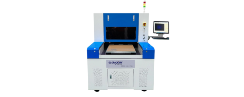
| Parameter | Specification | Why It Matters for OLED Glass |
|---|---|---|
| Laser type | UV Picosecond (355 nm) | Enables cold ablation; essential for OLED glass. |
| Pulse width | <10 ps | Eliminates thermal damage and particle generation. |
| Average power | 30W | High throughput for OLED panel production. |
| Processing accuracy | ≤20 µm | Meets the tight tolerances of OLED manufacturing. |
| X/Y repeatability | ±2 µm | Consistent part‑to‑part quality. |
| Working area | 600 mm × 500 mm | Supports mother glass panel processing. |
| Platform | Granite base + linear motors | Vibration‑free; long‑term precision. |
| CCD alignment | Auto‑recognition | Accurate cut placement; compensates for panel position. |
| Focus tracking | Dynamic Z‑axis | Maintains focus across the panel. |
| Gas management | Integrated nitrogen assist + vacuum extraction | Essential – keeps the glass surface clean. |
| Software | Self‑developed; DXF/DWG import | Rapid job changeover; process database. |
| Free solution
Previous: Can Laser Cut Glass? The Complete Guide to Precision Glass Laser Cutting
Next: Aluminosilicate Glass Laser Cutting – Precision Processing for Strengthened Cover Glass








