Key Words: Silicon Wafer Dicing PCB Depaneling Glass Cutting
Home > News > Industry News
【Description】:
Comprehensive guide on UV picosecond laser cutting for Polyimide (PI) film in flexible display manufacturing, covering process challenges, cold ablation physics, and panel singulation applications.
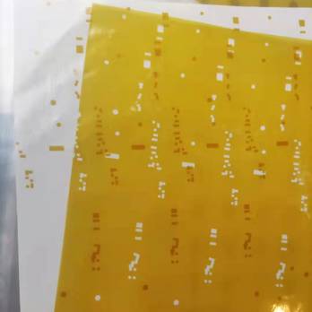
Polyimide (PI) film is the foundation upon which modern flexible displays are built. As the substrate material for flexible OLEDs, Polyimide provides the mechanical support, thermal stability, and flexibility required for foldable smartphones, rollable TVs, and curved automotive displays. Typically ranging from 10 to 50 micrometres in thickness—thinner than a human hair—PI enables displays to bend, fold, and roll without damage.
Cutting Polyimide film is a critical step in flexible display manufacturing. It occurs at multiple stages: cutting the film to panel size before deposition, singulating individual displays after fabrication, and trimming edges to final dimensions. The quality of these cuts directly impacts display yield, edge reliability, and fold durability.
PI film combines three material properties that create a perfect storm of processing difficulty:
| Challenge | Why It Matters | What Happens When Processing Fails |
|---|---|---|
| Extreme thinness (10–50 µm) | Any mechanical contact causes tearing or deformation. | Rough edges, delamination, edge deformation—defects that propagate during folding. |
| Heat sensitivity | PI chars, melts, or discolours when exposed to excess heat. | Charred edges, discolouration, loss of flexibility—defects that degrade display quality. |
| Transparency to IR wavelengths | IR lasers pass through PI without absorption—no cutting occurs. | Cannot cut—energy passes through the material. |
The triple sensitivity problem: PI is mechanically sensitive (any contact causes stress), thermally sensitive (any heat causes damage), and optically sensitive (wrong wavelength passes through). Any viable cutting method must be non‑contact, thermal‑free, and wavelength‑matched.
This combination of requirements eliminates most conventional cutting methods—mechanical cutting, CO₂ lasers, and IR fibre lasers—leaving only advanced laser solutions as viable options.
| Method | Why It Fails on PI |
|---|---|
| Mechanical die cutting | Requires high force—tears the thin film; creates rough edges and particles. |
| CO₂ laser (thermal) | Too much heat—causes charring, melting, and a large heat‑affected zone. |
| IR fibre laser (1064 nm) | No absorption—energy passes through without cutting. |
| UV nanosecond laser | Some thermal component remains—creates heat‑affected zone (10–30 µm) that can char or discolour PI. |
The conclusion: Only UV picosecond lasers deliver the combination of non‑contact, cold ablation, and clean processing that PI film requires.
Poor PI cutting is not just a cosmetic issue—it directly impacts display performance and yield:
| Defect | Consequence |
|---|---|
| Rough/torn edges | Compromises edge sealing—allows moisture ingress; reduces fold durability. |
| Charring / discolouration | Creates optical defects—affects display clarity and brightness. |
| Particle generation | Contaminates OLED layers—creates pixel defects; reduces yield. |
| Delamination | Separates PI from adjacent layers—device failure. |
| Stress concentration | Propagates during folding—causes edge cracking and device failure. |
UV picosecond laser cutting succeeds where other methods fail because it addresses the fundamental physics of PI processing:
The UV wavelength (355 nm) is strongly absorbed by PI—unlike IR, which passes through. This means the laser energy is deposited exactly where it is needed: at the material surface.
The picosecond pulse duration (<10 ps) is shorter than the time it takes for heat to diffuse into the surrounding material. The energy is confined to the focal spot, and the material is vaporised directly—bypassing the melt phase entirely.
The result is cold ablation: material removal with negligible heat transfer. The heat‑affected zone is virtually zero (<3 µm). The surrounding PI remains chemically and mechanically intact, with no charring, melting, or discolouration.
UV ps laser cutting delivers the combination of capabilities that flexible display manufacturing demands:
Smooth, clean edges – enabling reliable edge sealing and bonding.
Zero thermal damage – preserving PI properties and OLED layer integrity.
No mechanical stress – eliminating tearing and delamination risks.
Particle‑free surfaces – preventing pixel defects and maintaining high yield.
High precision – meeting the ±20 µm tolerances of display manufacturing.
High throughput – fast processing suitable for volume production.
PI film cutting is required at several critical stages of flexible display production:
| Manufacturing Stage | What Is Cut | Why Laser Cutting Is Essential |
|---|---|---|
| Panel singulation | PI film on carrier glass | Defines panel size before deposition—cut quality affects TFT and OLED alignment. |
| Final singulation | PI film after OLED fabrication | Separates individual displays—edge quality affects fold durability. |
| Edge trimming | PI edges after singulation | Removes irregular edges—provides clean, straight edges for assembly. |
| Notch / hole cutting | PI film for camera holes, speaker cutouts | Precision cutting—any roughness creates defects. |
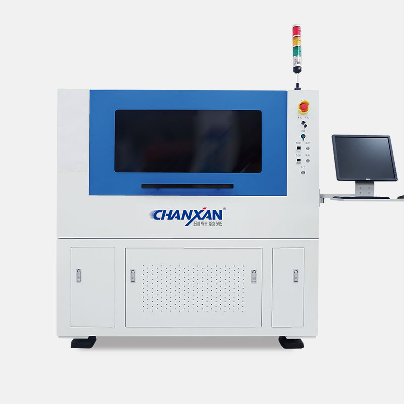
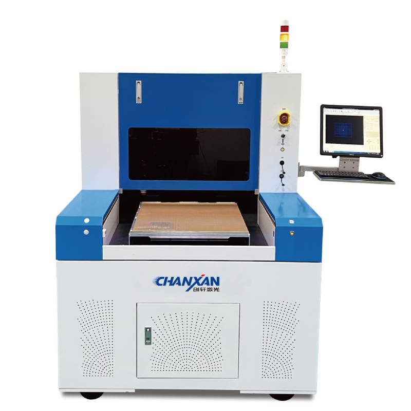
Chanxan Laser offers a comprehensive UV picosecond laser system specifically designed for PI film cutting and flexible display processing:
| Feature | What It Delivers for PI Cutting |
|---|---|
| Laser type: UV Picosecond (355 nm, <10 ps) | Clean, crack‑free edges—no charring, no melting, no delamination. |
| Non‑contact processing | No mechanical stress—no tearing, no deformation. |
| Integrated nitrogen assist + vacuum | Particle‑free surfaces—critical for OLED yield. |
| 600×500 mm working area | Panel‑scale processing—supports large‑format flexible displays. |
| ≤20 µm accuracy / ±2 µm repeatability | Meets display tolerances—consistent part‑to‑part quality. |
| Software‑defined cutting paths | Any shape—straight lines, curves, notches, holes. |
Chanxan Laser provides the production‑ready UV ps solutions. With deep process expertise, advanced system engineering, and a global support network, Chanxan is a trusted partner for display manufacturers worldwide.
| Free solution
Previous: UV Picosecond Laser for OLED Processing – The Enabling Technology for Advanced Display Manufacturing
Next: Flexible OLED Laser Cutting – Precision Processing for Foldable and Rollable Displays