

Key Words: Silicon Wafer Dicing PCB Depaneling Glass Cutting
Home > News > Industry News
【Description】:
Comprehensive guide on UV picosecond laser technology in OLED manufacturing, covering cold ablation physics, UTG cutting, PI film processing, carrier glass cutting, and TGV drilling.
OLED displays have revolutionised the consumer electronics industry—offering superior contrast, faster response times, and enabling entirely new form factors such as foldable smartphones and rollable displays. However, the manufacturing processes behind these advanced displays impose extraordinary demands.
The materials used in OLED manufacturing—ultra‑thin glass (UTG) down to 20 µm, polyimide (PI) films, and heat‑sensitive organic layers—are fragile, thermally sensitive, and intolerant of mechanical stress. Conventional mechanical cutting introduces micro‑cracks and edge chipping. Thermal lasers generate heat‑affected zones that degrade material integrity. Both lead to catastrophic failure during folding or compromised display quality.
UV picosecond laser technology has emerged as the essential enabling solution. Its unique combination of short wavelength (355 nm) and ultra‑short pulse duration (<10 ps) delivers cold ablation—material removal with negligible heat transfer—making UV picosecond lasers the viable tool for many critical OLED fabrication steps.
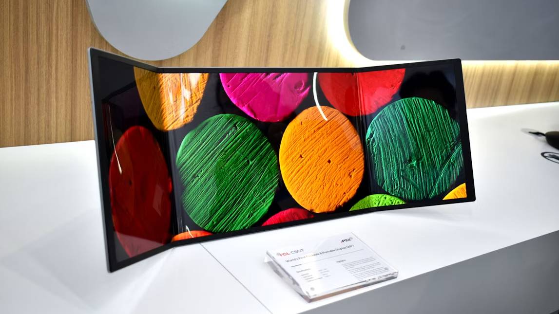
OLED displays are built from multiple layers of materials that are fundamentally difficult to process:
| Material | Role in OLED | Critical Property | Processing Challenge |
|---|---|---|---|
| Ultra‑Thin Glass (UTG) | Cover layer providing scratch resistance and optical clarity | 20–100 µm thick; chemically strengthened | Extremely brittle—any mechanical contact causes fracture; thermal stress shatters the glass |
| Polyimide (PI) | Flexible substrate for the entire display stack | 10–50 µm thick; heat‑sensitive | Thin and fragile—mechanical cutting tears the film; heat causes melting or charring |
| Carrier Glass | Temporary support during OLED fabrication | 0.3–0.7 mm thick | Must be cut cleanly without chipping—edge defects compromise subsequent processing |
| OLED Organic Layers | Light‑emitting stack | <1 µm thick; extremely heat‑sensitive | Any thermal damage creates pixel defects—reduces yield and display quality |
OLED materials share three forms of sensitivity that make conventional processing methods unacceptable:
| Sensitivity | Why It Matters | Which Materials Are Affected |
|---|---|---|
| Mechanical sensitivity | Contact forces cause chipping, cracking, or tearing—defects that propagate during folding or thermal cycling | UTG, PI, thin glass |
| Thermal sensitivity | Heat input degrades material properties—UTG loses compressive strength; PI melts or chars; OLED layers degrade | UTG, PI, OLED organic layers |
| Particle sensitivity | Contamination creates pixel defects—any particle >1 µm can render a pixel non‑functional | All OLED materials |
The conclusion: Any viable cutting method must be non‑contact (eliminating mechanical stress), thermal‑free (eliminating heat damage), and particle‑free (eliminating contamination).
Only UV picosecond lasers meet all three requirements.
The choice of 355 nm (UV) wavelength is fundamental to successful OLED processing:
| Wavelength | Interaction with OLED Materials | Result |
|---|---|---|
| IR (1064 nm) | Passes through transparent materials—no absorption | Cannot cut glass or PI effectively |
| Green (532 nm) | Moderate absorption | Limited effectiveness; some heat generation |
| UV (355 nm) | Strong absorption in glass, PI, and most OLED materials | Clean, efficient material removal |
| Deep UV (266 nm) | Very strong absorption | Effective but commercially limited |
Why UV matters: UV photons have high energy (3.5 eV), enabling direct photochemical bond breaking in materials. This is fundamentally different from IR processing, which relies on heating. The UV wavelength ensures that energy is absorbed where it is needed—at the material surface—not transmitted through the substrate.
The pulse duration determines whether heat has time to diffuse into the surrounding material. For OLED processing, heat diffusion is the enemy.
| Pulse Duration | Heat Diffusion | Processing Result |
|---|---|---|
| Nanosecond | Heat diffuses 3–5 µm | Creates a measurable heat‑affected zone—thermal damage |
| Picosecond | Heat diffuses <0.1 µm | Negligible heat‑affected zone—cold ablation |
| Femtosecond | Heat diffuses <0.02 µm | Ultra‑cold ablation—but slower and costlier |
Why picosecond is optimal: With <10 ps pulse duration, the laser energy is deposited faster than heat can diffuse into the surrounding material. This creates a cold ablation regime where material is removed with minimal thermal impact—critical for heat‑sensitive OLED layers and thin substrates.
Cold ablation is the combination of UV wavelength and picosecond pulse duration:
| Mechanism | Effect | Benefit for OLED |
|---|---|---|
| Photochemical bond breaking | UV photons directly break molecular bonds | Minimal heat generation |
| Plasma formation | Material is converted directly from solid to plasma | Clean removal without melting |
| No melt phase | Material bypasses liquid state | No recast layer—clean edges |
| Negligible heat diffusion | Pulse duration < heat diffusion time | No heat‑affected zone—preserves OLED integrity |
The result: A cutting process that removes material with no thermal damage, no mechanical stress, and no particle contamination—exactly what OLED manufacturing requires.
Ultra‑Thin Glass (UTG) is the cover material that makes foldable displays possible. It must be cut without any edge defects—chips or micro‑cracks—because these defects propagate during folding, causing device failure.
Why UV ps is essential for UTG:
UTG is chemically strengthened (compressive surface layer).
Any thermal input reduces surface compression, weakening the edge.
Any mechanical force induces shattering—UTG cannot tolerate contact.
Only UV ps cold ablation removes material without heat or force, preserving the strengthened layer and achieving >200,000 fold cycles.
The alternative view: Manufacturers who attempt mechanical scribing or CO₂ laser cutting of UTG experience yield losses >80%—making UV ps laser cutting not just the best option, but the only economically viable one.
Polyimide (PI) film serves as the flexible substrate for OLED displays. It must be cut cleanly without thermal damage or delamination.
Why UV ps is essential for PI:
PI is thin (10–50 µm) and fragile—mechanical cutting tears the material.
PI is heat‑sensitive—thermal lasers cause charring or melting.
UV ps processing produces clean, smooth edges without thermal damage or tearing.
The cold ablation mechanism ensures that the PI remains intact, with no delamination from adjacent layers.
The alternative view: Mechanical cutting creates rough edges and tear—defects that compromise the structural integrity of the flexible display. CO₂ or IR lasers cause charring and melting—defects that degrade optical performance.
Carrier glass provides mechanical support during OLED fabrication. After deposition, the carrier glass must be cut to separate individual panels or to prepare for laser lift‑off.
Why UV ps is essential for carrier glass:
Glass is brittle—mechanical cutting causes chipping and cracking.
Thermal cutting creates a heat‑affected zone that weakens the glass.
UV ps cutting produces clean, chip‑free edges with minimal HAZ, ensuring that the glass maintains its structural integrity.
The alternative view: Mechanical cutting of carrier glass creates chipping that can damage adjacent OLED layers during separation. CO₂ laser cutting creates thermal stress that can cause glass fracture.
Through‑Glass Via (TGV) drilling is essential for advanced OLED packaging, enabling electrical connections through the glass substrate.
Why UV ps is essential for TGV:
Glass requires high peak power for nonlinear absorption—UV ps delivers the necessary intensity.
The short pulse width ensures minimal thermal damage to the glass.
UV ps enables high‑aspect‑ratio vias with smooth sidewalls.
The alternative view: Mechanical drilling of glass creates micro‑cracks and is limited to low aspect ratios. Thermal drilling creates rough sidewalls with significant thermal damage.
Laser Lift‑Off is the critical process that separates the flexible OLED display from the carrier glass after fabrication.
Why UV ps is essential for LLO:
The laser must pass through transparent carrier glass and be absorbed at the PI‑glass interface.
UV ps provides the precise energy control needed for uniform separation.
Cold ablation ensures that neither the PI nor the OLED layers are thermally damaged during separation.
The alternative view: LLO requires a laser with precise wavelength, pulse duration, and beam uniformity—UV ps offers the control and consistency necessary for high‑yield LLO.
Chanxan Laser is a leading manufacturer of advanced laser processing systems in China, offering comprehensive solutions for OLED manufacturing. With over 100 patents, ISO9001, FDA, and CE certifications, and a global service network spanning 100+ countries, Chanxan delivers the precision, reliability, and process expertise that display manufacturers require.
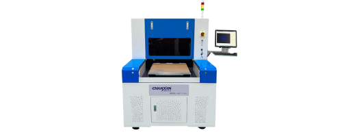
The Chanxan UV Picosecond Laser System is purpose‑built for the demanding requirements of OLED processing. It combines a high‑power UV picosecond laser source with precision motion control, advanced beam delivery, and integrated cleanliness management.
Cold ablation — zero thermal damage, zero micro‑cracks, zero charring.
High precision — ±2 µm repeatability, ≤20 µm processing accuracy.
Clean processing — integrated nitrogen assist and vacuum extraction—particle‑free surfaces.
Panel‑scale capability — 600×500 mm working area supporting large‑format OLED panels.
Multi‑function flexibility — cutting, drilling, marking, and grooving on a single platform.
Chanxan Laser is committed to advancing display manufacturing technology through continuous innovation in ultrafast laser processing. The company's experience across multiple industries—including consumer electronics, semiconductors, and medical devices—provides a deep foundation of knowledge that benefits every OLED customer.
| Free solution
Previous: Precision Laser Processing of Thin Films: Technologies, Applications, and Equipment Solutions
Next: PI Film Laser Cutting for Flexible Displays – A Complete Guide to Processing the Polyimide Substrate








