Key Words: Silicon Wafer Dicing PCB Depaneling Glass Cutting
Home > News > Industry News
【Description】:
A comprehensive guide on laser cutting technologies for flexible OLED display manufacturing, including PI film cutting, Laser Lift-Off (LLO), and Ultra-Thin Glass (UTG) cutting.
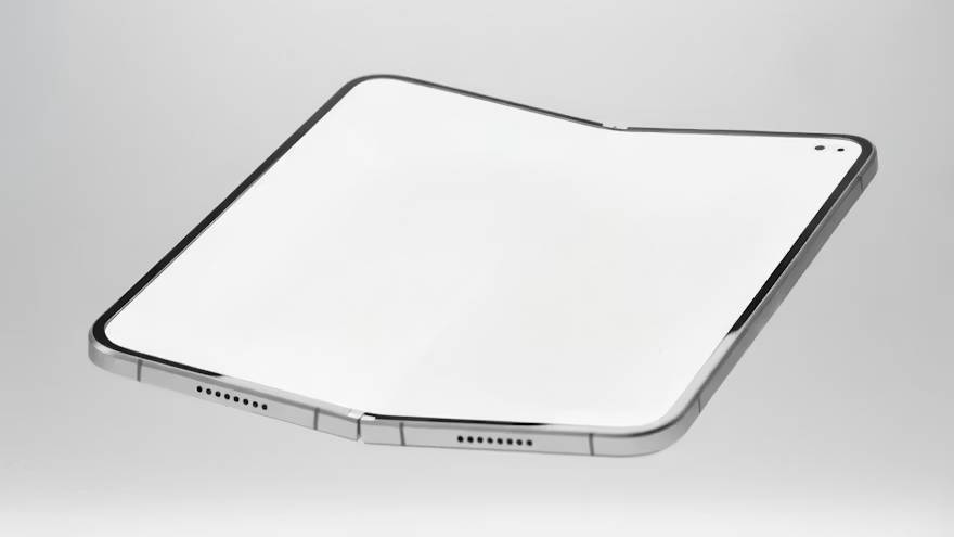
The display industry has undergone a dramatic transformation over the past decade. Rigid glass‑based displays, which dominated the market for years, are increasingly being complemented—and in some cases replaced—by flexible OLED (FOLED) displays. These devices, found in foldable smartphones, rollable TVs, curved automotive displays, and wearable electronics, offer unprecedented design freedom and user experience.
Flexible OLED displays are fundamentally different from their rigid counterparts. They are built on flexible substrates—typically polyimide (PI) films or ultra‑thin glass (UTG)—that enable bending, folding, and rolling without damaging the delicate organic light‑emitting layers.
Ultrafast laser technology—specifically UV picosecond (ps) and femtosecond (fs) lasers—has emerged as the only industrial‑viable solution for flexible OLED cutting. Its cold ablation mechanism delivers crack‑free, stress‑free, and particle‑free cuts, enabling the high yields required for commercial production.
A flexible OLED display consists of multiple thin layers deposited on a flexible substrate:
| Layer | Material | Thickness | Function |
|---|---|---|---|
| Carrier substrate | Glass (for processing) | 0.3–0.7 mm | Provides mechanical support during deposition—removed after fabrication. |
| Flexible substrate | Polyimide (PI) | 10–50 µm | The actual display base—remains in the final product. |
| TFT backplane | a‑Si, LTPS, IGZO | <1 µm | Controls pixel switching. |
| OLED stack | Organic layers | <1 µm | Emits light—highly sensitive to heat and particles. |
| Encapsulation | Thin‑film encapsulation (TFE) | <5 µm | Protects organic layers from moisture and oxygen. |
| Cover layer | UTG or hard coating | 20–100 µm | Protects the display surface—provides scratch resistance and optical clarity. |
| Substrate | Typical Thickness | Cutting Challenge | Why Laser Is Essential |
|---|---|---|---|
| Polyimide (PI) film | 10–50 µm | Thin, flexible, heat‑sensitive—mechanical cutting causes tearing and deformation. | Cold ablation removes material without heat; no mechanical stress. |
| Carrier glass | 0.3–0.7 mm | Glass is brittle—mechanical cutting causes chipping and cracking. | Laser cutting is non‑contact; cold ablation preserves edge strength. |
| Ultra‑Thin Glass (UTG) | 20–100 µm | Extremely fragile—cannot tolerate mechanical contact or thermal stress. | UV ps laser cutting is the only method that yields crack‑free edges. |
| Encapsulation layers | <5 µm | Thin films—must be cut without damaging the underlying organic layers. | Precise depth control—laser stops at the target layer. |
Flexible OLEDs are not manufactured directly on the PI film alone. Instead, the PI is first coated onto a rigid carrier glass substrate. The entire display stack is then fabricated on the carrier glass using standard deposition and lithography equipment. After fabrication, the flexible display is separated from the carrier glass—a critical step known as laser lift‑off (LLO).
Cutting processes occur at multiple stages:
| Stage | Process | Material Cut | Laser Required |
|---|---|---|---|
| Before LLO | Cutting the panel on the carrier glass | PI + carrier glass | Yes – UV ps |
| After LLO | Final singulation of flexible displays | PI film | Yes – UV ps |
| UTG lamination | Cutting UTG cover glass | UTG (20–100 µm) | Yes – UV ps |
| Cell singulation | Separating multiple displays from a large panel | PI + TFT + OLED stack | Yes – UV ps |
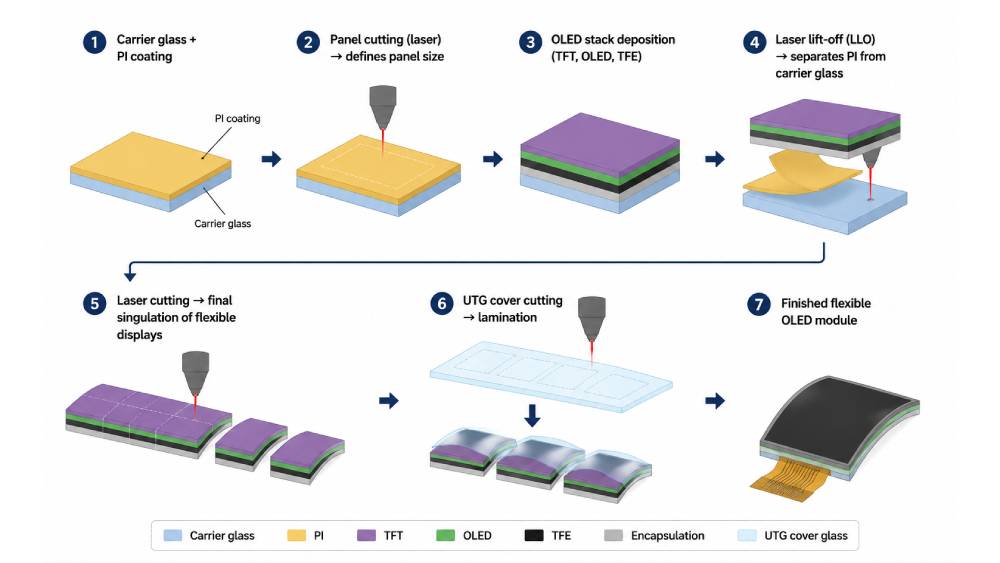
Purpose: The PI film is cut to the required panel size before deposition or as part of the panel singulation process.
| Parameter | Typical Value | Why It Matters |
|---|---|---|
| Material | Polyimide film (10–50 µm) on glass carrier. | Thin film—requires minimal heat input. |
| Laser type | UV picosecond (355 nm) | Cold ablation—no charring or thermal stress. |
| Cut quality | Clean edges, no delamination. | PI must remain intact for subsequent deposition. |
| Kerf width | <20 µm | Minimises material loss. |
Purpose: LLO is a critical step that separates the completed flexible display from the carrier glass. A laser beam is directed through the transparent carrier glass and absorbed at the PI‑glass interface, causing the PI to release.
| Parameter | Typical Value | Why It Matters |
|---|---|---|
| Material | PI‑glass interface. | The laser must be absorbed at the interface, not in the glass. |
| Laser type | UV laser (355 nm) or excimer laser. | The wavelength must pass through glass and be absorbed by PI. |
| Beam profile | Line beam (top‑hat profile). | Uniform energy distribution—prevents delamination defects. |
| Process | Scanning the beam across the entire panel. | Entire panel is released in one process. |
Key requirement: The laser must be absorbed at the PI‑glass interface without damaging the PI or the OLED layers. This requires precise control of laser fluence and beam uniformity.
Purpose: After LLO, the individual flexible displays are cut from the PI film to final dimensions.
| Parameter | Typical Value | Why It Matters |
|---|---|---|
| Material | PI film (10–50 µm) + TFT + OLED stack. | The OLED layers are sensitive to heat and particles. |
| Laser type | UV picosecond (355 nm) | Cold ablation—no HAZ; no charring; no particles. |
| Cut quality | Smooth, crack‑free edges. | Edge defects can propagate during folding. |
| Throughput | High | Each display must be cut quickly—production volume is high. |
Purpose: UTG (ultra‑thin glass) is used as a cover layer for flexible OLED displays, providing scratch resistance and optical clarity.
| Parameter | Typical Value | Why It Matters |
|---|---|---|
| Material | UTG (20–100 µm) | Extremely fragile—must be cut without mechanical contact. |
| Laser type | UV picosecond (355 nm) | Non‑contact, cold ablation—preserves glass strength. |
| Cut quality | Crack‑free, chip‑free edges. | Edge defects reduce fold endurance (<200,000 cycles). |
| Shape | Rectangles, curves, camera holes, notches. | Software‑defined cutting—no tooling changes. |
| Aspect | Flexible OLED Cutting | Rigid Glass Cutting |
|---|---|---|
| Substrate | PI film, UTG, carrier glass | Glass panel (0.3–0.7 mm) |
| Thickness | 10–100 µm (PI, UTG) | 0.3–0.7 mm |
| Sensitivity | Extremely high – heat, stress, particles damage OLED layers | Moderate – chipping and cracking are the main concerns |
| Laser type | UV ps (mandatory for PI and UTG) | UV ps, CO₂, or mechanical (for thick glass) |
| Edge quality | Absolute requirement – defects reduce fold endurance | Important – but less critical than flexible |
| Post‑processing | None – direct assembly | Edge grinding/polishing optional |
| Key driver | Fold durability and yield | Speed and cost |
Chanxan Laser provides the production‑ready solutions that make flexible OLED manufacturing possible. The UV Picosecond Laser System delivers the precision, speed, and reliability that display manufacturers demand—enabling the foldable devices of today and the rollable displays of tomorrow.
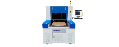
| Feature | Specification | Why It Matters |
|---|---|---|
| Laser type | UV Picosecond (355 nm) | Cold ablation—preserves OLED layers; ensures fold durability. |
| Pulse width | <10 ps | Eliminates thermal damage—no HAZ, no charring. |
| Average power | 30W | High throughput—fast cutting of flexible display panels. |
| Processing accuracy | ≤20 µm | Meets display tolerances. |
| X/Y repeatability | ±2 µm | Consistent part‑to‑part quality. |
| Working area | 600×500 mm | Supports large panels—high utilisation. |
| CCD alignment | Auto‑recognition | Compensates for panel position—accurate registration. |
| Focus tracking | Dynamic Z‑axis | Maintains focus across warped panels—consistent edge quality. |
| Gas & extraction | Nitrogen assist + vacuum | Removes debris—zero particle contamination. |
| Software | Self‑developed; DXF/DWG import | Rapid job changeover; process database. |
| Free solution
Previous: PI Film Laser Cutting for Flexible Displays – A Complete Guide to Processing the Polyimide Substrate
Next: Laser Processing in OLED Manufacturing: Technologies & Equipment Guide