
Key Words: Silicon Wafer Dicing PCB Depaneling Glass Cutting
Home > News > Industry News
【Description】:
An in-depth technical comparison between picosecond (ps) lasers and traditional nanosecond or CW lasers, covering pulse duration, peak intensity, heat diffusion, thermal-affected zones, and applications.
When engineers compare laser tools for manufacturing, the term "traditional laser" usually refers to nanosecond (ns) pulsed lasers and continuous-wave (CW) or quasi-continuous lasers—the workhorses that have dominated industrial marking, welding, cutting, and drilling for decades. Picosecond (ps) lasers belong to the ultrafast laser family, with pulse durations roughly between 1 and 100 ps. The difference is not just a number on a datasheet. It changes how energy is deposited into a material, what happens to the surrounding region, and which applications become feasible. This article explains the physical differences, the practical consequences, and where each technology still wins.
The most obvious difference is pulse duration. A typical nanosecond laser has pulses of 1–100 ns. A picosecond laser has pulses of 1–100 ps—roughly one thousand times shorter. A femtosecond laser is shorter still, but that is a separate comparison.
Pulse duration determines peak power for a given pulse energy. If a 10 µJ pulse is compressed from 10 ns to 10 ps, the peak power rises by a factor of about 1,000. This is the core of the difference. Picosecond pulses reach very high peak intensities at modest pulse energies, which drives nonlinear absorption processes rather than simple linear heating.
During a laser pulse of duration $\tau$, heat diffuses a characteristic distance $L \approx \sqrt{D\tau}$, where $D$ is the thermal diffusivity of the material. This single relationship explains most of the practical differences.
For silicon, $D$ is roughly 0.8 cm²/s. A 10 ns pulse allows heat to diffuse about 0.9 µm; a 10 ps pulse limits diffusion to about 28 nm. For glass, with $D$ around 0.008 cm²/s, a 10 ns pulse gives about 90 nm of diffusion, while a 10 ps pulse gives about 9 nm. For sapphire, with $D$ around 0.12 cm²/s, the values are roughly 350 nm for 10 ns and 11 nm for 10 ps.
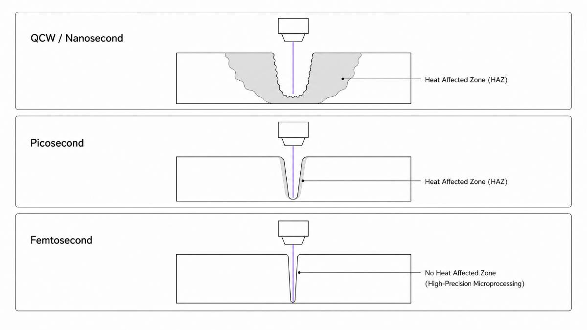
In practical terms, a nanosecond pulse has time to heat a micrometer-scale region around the spot before the material leaves. A picosecond pulse deposits energy so quickly that the material is removed or modified before significant heat escapes into the surroundings. This is why picosecond processing is often described as cold ablation or low-thermal-damage processing.
Nanosecond lasers remove material primarily through heating. The absorbed energy raises the local temperature until the material melts, vaporizes, or is ejected by recoil pressure. This is effective and efficient for many metals and polymers, and it is the basis of most industrial laser cutting, welding, and marking.
The side effects are well known. The heat-affected zone (HAZ) can extend micrometers beyond the cut. Molten material can be ejected and resolidify as recast or dross. Microcracks can form, especially in brittle materials. For semiconductors, low-k dielectrics, and transparent materials, these effects limit yield and require post-processing such as etching, polishing, or cleaning.
Nanosecond lasers are not obsolete. They are often cheaper, more electrically efficient, and available at higher average power. For thick metal cutting, welding, and many marking applications, they remain the best choice.
Picosecond lasers remove material through a different pathway. The high peak intensity drives multiphoton absorption and avalanche ionization, creating a dense free-electron plasma. The material is then ejected through phase explosion, Coulomb explosion, or direct vaporization. Because the energy is deposited in a very short time, the surrounding lattice does not have time to heat significantly.
The practical results are:
Smaller HAZ: Typically sub-micrometer, often tens of nanometers.
Less recast: Reduced molten layer and dross.
Fewer microcracks: Important for brittle materials such as SiC, GaN, sapphire, and glass.
Cleaner sidewalls: Less post-processing required.
Better feature control: Narrower kerfs and more precise drilling.
Transparent material processing: Nonlinear absorption allows internal modification of glass and sapphire, enabling stealth dicing and filamentation-based cutting.
The trade-offs are also real. Picosecond lasers generally cost more, have lower wall-plug efficiency, and can have lower average power than nanosecond sources. Throughput can be lower unless burst mode, multibeam processing, or higher-power sources are used.
| Aspect | Traditional Nanosecond Laser | Picosecond Laser |
|---|---|---|
| Pulse duration | 1–100 ns | 1–100 ps |
| Peak power (same pulse energy) | Lower | ~1,000× higher |
| Material removal mechanism | Heating, melting, vaporization | Nonlinear absorption, cold ablation |
| Heat-affected zone | Micrometer scale | Sub-micrometer to tens of nanometers |
| Recast and dross | Often significant | Minimal |
| Microcracking | Common in brittle materials | Reduced |
| Kerf width | Wider | Narrower |
| Transparent material processing | Limited; often surface or stress-driven | Effective; internal modification possible |
| Capital cost | Lower | Higher |
| Wall-plug efficiency | Higher | Lower |
| Average power | Higher | Generally lower, improving |
| Throughput | High for simple cuts | Improving with burst mode and multibeam |
| Typical applications | Metal cutting, welding, marking, some dicing | SiC/GaN dicing, sapphire/glass cutting, TGV, thin wafer dicing, precision drilling |
Nanosecond lasers can dice wafers, but the HAZ and microcracks can reduce die strength and yield, especially for SiC, GaN, and thin wafers. Picosecond lasers reduce these defects, which is why they are increasingly used for laser grooving and stealth dicing. The green benefit is higher yield and less material waste.
Nanosecond lasers tend to generate stress and uncontrolled cracking in transparent brittle materials. Picosecond lasers can modify the material internally through nonlinear absorption, enabling clean separation with minimal edge damage. This is important for smartphone camera covers, smartwatch crystals, and display glass.
For TSVs, TGVs, and microvias, nanosecond lasers can produce larger HAZ and recast, requiring additional etching. Picosecond lasers can produce cleaner sidewalls and more controllable taper, though some hybrid processes still use wet etching to finish the via.
This is where nanosecond and CW lasers remain dominant. For thick metal sections, welding, and high-throughput cutting, the higher average power and lower cost of traditional lasers usually win. Picosecond lasers are used for thin foils, precision stents, and dissimilar material processing where HAZ matters.
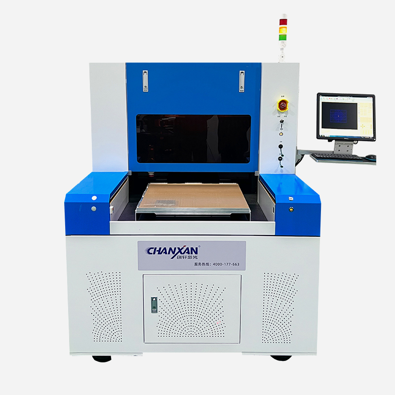
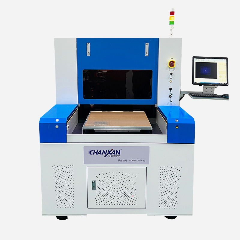
Chanxan Laser is a laser technology company specializing in ultrafast and picosecond laser systems for precision micromachining. Its product portfolio typically covers picosecond laser sources, galvo scanning systems, and integrated processing platforms designed for semiconductor, electronic, and advanced materials applications. In the comparison between picosecond and traditional lasers, systems in this class are positioned to support cutting, drilling, and dicing processes where low thermal damage, fine feature control, and stable long-term operation are required.
The difference between picosecond and traditional lasers comes down to time. Nanosecond lasers deposit energy over a timescale that allows heat to spread, melt, and resolidify material. Picosecond lasers deposit energy faster than heat can diffuse, enabling nonlinear absorption and cold ablation. This produces smaller HAZ, less recast, fewer microcracks, and cleaner features—advantages that matter most for hard, brittle, and transparent materials. Traditional lasers remain superior for high-power metal cutting, welding, and many marking applications. The right choice depends on material, quality requirements, throughput, and cost. As picosecond technology improves in power and throughput, the boundary between the two continues to shift.
Discover how Chanxan Laser's advanced picosecond systems deliver zero thermal damage and high-precision results for your application.
Contact to Get a Consultation| Free solution
Previous: UV Nanosecond Lasers for PI Heating Film Precision Cutting
Next: Sapphire and Glass Cutting with Picosecond Lasers: From Smartphones to Wearables