
Key Words: Silicon Wafer Dicing PCB Depaneling Glass Cutting
Home > News > Industry News
【Description】:
Explore how picosecond lasers revolutionize sapphire and glass cutting for smartphones, wearables, and consumer electronics, offering high precision and minimal thermal damage.
Picosecond lasers are moving from laboratory research into high-volume semiconductor manufacturing. As devices become thinner, more fragile, and more highly integrated, traditional mechanical dicing and nanosecond laser processing often struggle with chipping, microcracks, heat-affected zones (HAZ), and yield loss. With pulse durations roughly between 1 and 100 ps, picosecond lasers occupy a practical middle ground between nanosecond and femtosecond sources: they offer relatively cold ablation, high precision, and industrially useful throughput. For cutting, drilling, and dicing in semiconductor manufacturing, they are becoming an important micromachining solution.
The key advantage of picosecond lasers is the time scale. For a material with thermal diffusivityD, the approximate heat diffusion length during a pulse of durationτ isL≈Dτ. For silicon, withD on the order of 0.8 cm²/s, a 10 ps pulse gives a diffusion length of only tens of nanometers, while a 100 ns pulse can reach the micrometer range. This means picosecond lasers can remove or modify material before significant heat spreads into the surrounding region, reducing the heat-affected zone, recast layer, and microcracking.
The material removal mechanism typically involves multiphoton absorption, avalanche ionization, phase explosion, and direct vaporization or modification. It is not perfectly “cold,” but it is often described as cold ablation or low-thermal-damage processing. Common wavelengths include UV 355 nm, green 532 nm, and IR 1064 nm. UV is preferred for surface absorption and small features, green offers a balance of absorption and efficiency, and IR is widely used for internal modification and stealth dicing.
In picosecond laser cutting applications, picosecond lasers are especially suitable for brittle semiconductors and composite substrates such as SiC, GaN, sapphire, glass, and thin silicon. SiC power devices are hard and brittle, and mechanical blade dicing can cause chipping and cracks. Picosecond lasers can reduce mechanical stress through local ablation or internal modification, improving die strength. GaN is often grown on sapphire, Si, or SiC substrates, where heteroepitaxial stress is high; laser cutting can help suppress crack propagation.
For glass and composite substrates, picosecond lasers can be combined with Bessel beams, multifocus optics, or burst mode to create high-aspect-ratio modified zones, which are then separated by tape expansion or etching. Cutting quality is usually evaluated by SEM inspection of the HAZ, microcracks, and kerf, and by Raman spectroscopy for residual stress. The actual process window depends on wavelength, pulse energy, repetition rate, scan speed, and material thickness, and must be validated case by case.
In picosecond laser drilling, picosecond lasers are used for through-silicon vias (TSVs), through-glass vias (TGV), MEMS microholes, and packaging microvias. TSV production is still dominated by DRIE, but lasers can be used for pre-drilling, trimming, or glass via formation. Picosecond laser drilling can produce relatively clean sidewalls, controllable taper, and fewer microcracks. A subsequent chemical etch can remove the damaged layer and create a cleaner via.
TGV is a key structure for glass interposers and RF packaging. Picosecond lasers can create high-aspect-ratio modifications or ablations in glass, which are then enlarged by wet etching. The main challenges are taper control, chipping, particles, and throughput. Burst mode and multibeam parallel processing can improve efficiency, but thermal accumulation and sidewall quality must be balanced.
In picosecond laser dicing, picosecond lasers are used in three main routes: laser ablation dicing, laser grooving plus blade dicing, and stealth dicing. For low-k dielectrics, passivation layers, and metal layers, direct blade dicing can cause delamination and chipping. Picosecond laser grooving before blade dicing can significantly improve yield. For thin wafers, stealth dicing uses a transparent wavelength to form an internal modified layer, followed by tape expansion for separation, resulting in less debris and a narrower kerf.
Picosecond lasers are also used in dicing before grinding (DBG) and thin-chip separation. Compared with nanosecond lasers, they generally reduce HAZ and microcracks; compared with femtosecond lasers, they offer lower cost and higher throughput. The final choice depends on material, thickness, die strength requirements, and production targets.
Picosecond lasers are not a universal replacement in semiconductor manufacturing. They still face particle contamination, taper control, aspect-ratio limits, equipment cost, throughput bottlenecks, and inline monitoring challenges. Future trends include burst mode and adaptive pulse control, Bessel beams and multifocus parallel processing, AI-assisted process window optimization, in-situ monitoring, and hybrid integration with blade dicing, DRIE, and wet etching.
Overall, picosecond lasers provide a balanced combination of low thermal damage, high precision, and broad material adaptability for cutting, drilling, and dicing. For difficult materials such as SiC, GaN, glass, low-k dielectrics, and thin wafers, they are becoming a key tool for improving yield and reliability. Equipment documentation, material data, and high-volume validation should determine specific parameters and process routes.
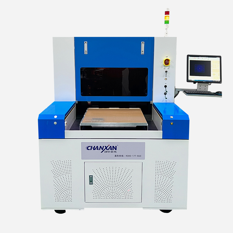
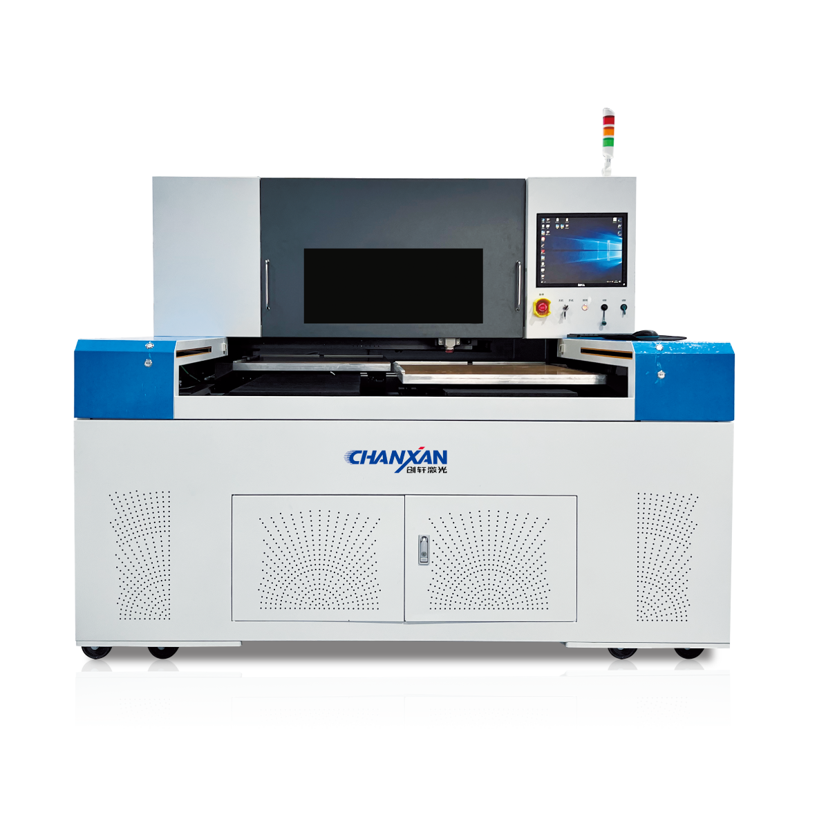
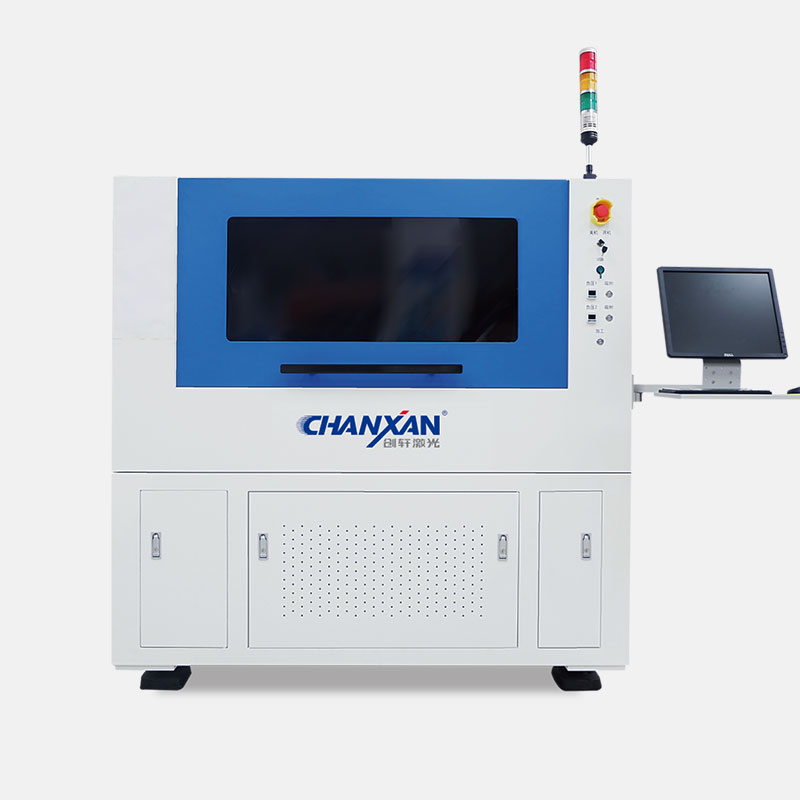
Chanxan Laser is a laser technology company specializing in ultrafast and picosecond laser systems for precision micromachining. Its product portfolio typically covers picosecond laser sources, galvo scanning systems, and integrated processing platforms designed for semiconductor, electronic, and advanced materials applications. In the context of semiconductor manufacturing, Chanxan Laser's systems are positioned to support cutting, drilling, and dicing processes where low thermal damage, fine feature control, and stable long-term operation are required.
For cutting, Chanxan Laser's picosecond platforms can be configured with UV, green, or IR wavelengths to match different material absorption characteristics. This flexibility is useful for processing SiC, GaN, sapphire, glass, and thin silicon, where the optimal wavelength and pulse parameters vary significantly. For drilling, its systems can be adapted for TSV, TGV, and microvia formation, often with burst mode or multibeam options to improve throughput and sidewall quality. For dicing, Chanxan Laser offers laser grooving and stealth dicing solutions that can be integrated with blade dicing or tape expansion lines, helping reduce chipping and improve die strength.
Connect with our experts to find the tailored picosecond laser processing solution for your application.
Contact to Get a Consultation| Free solution
Previous: Picosecond Laser vs. Traditional Laser: What's the Difference?
Next: Picosecond Lasers in Semiconductor Manufacturing: Cutting, Drilling, and Dicing