Key Words: Silicon Wafer Dicing PCB Depaneling Glass Cutting
Home > News > Industry News
【Description】:
Discover Chanxan's picosecond laser wafer dicing machine for advanced packaging glass substrates. Features <3μm HAZ, <5μm kerf, and micro-crack-free TGV processing.
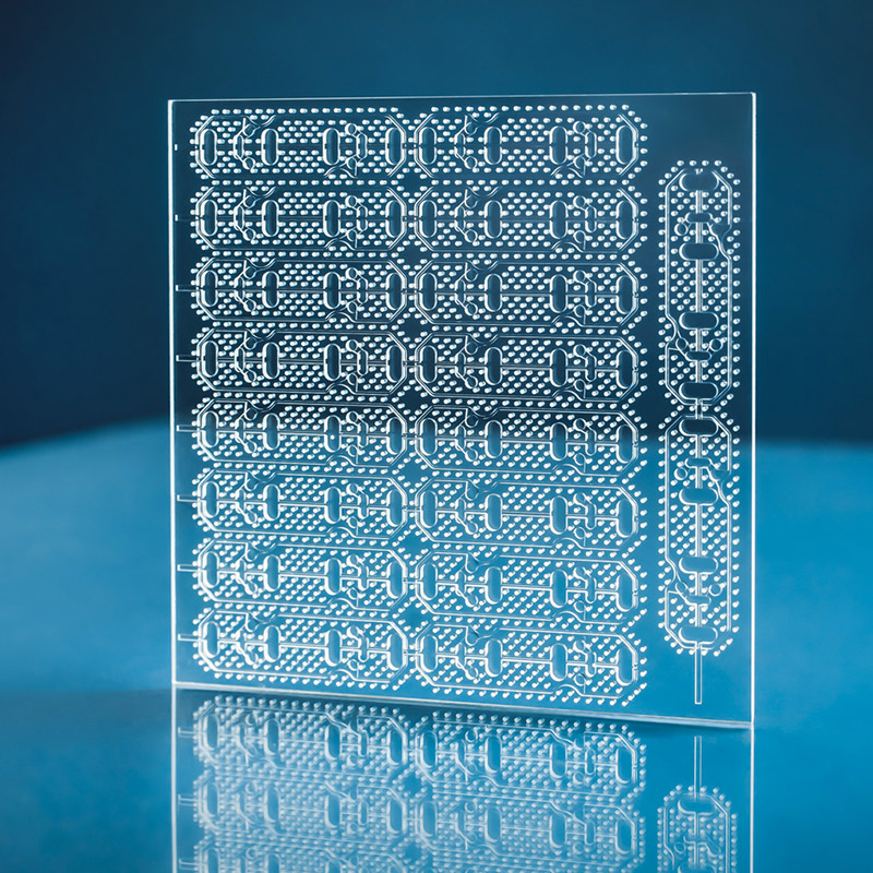
In the realm of advanced packaging and high-performance computing, glass wafers have become pivotal. They are increasingly utilized in 2.5D/3D interposers leveraging Through Glass Vias (TGV), which offer superior electrical performance and thermal stability compared to traditional silicon. Additionally, they serve as crucial carriers or substrates in Fan-out Wafer-Level Packaging (FOWLP) and enable the high-density integration of Integrated Passive Devices (IPD), significantly optimizing RF and high-frequency circuit designs.
The dicing challenge:
Unlike silicon, glass is an amorphous, brittle material with:
No plastic deformation regime — it fractures catastrophically above its elastic limit
High sensitivity to thermal gradients — localized heating creates tensile stress and micro-cracks
Variable composition — from fused silica (SiO₂) to borosilicate, aluminosilicate, and other specialized glasses
Surface defects from previous processing steps propagate during dicing
Conventional dicing methods fail for glass wafers:
Blade dicing generates cracks, edge chipping, and micro-fractures that propagate unpredictably. Blade life is also short due to the glass's hardness.
Nanosecond laser dicing creates significant heat-affected zones (10–30 μm) with thermal micro-cracks. The re-solidified glass along the cut edge has altered optical and mechanical properties.
Water jet cutting is unsuitable for fine-pitch singulation and leaves surface contamination.
For advanced packaging, where glass substrates must maintain their structural integrity through multiple assembly steps (including Cu metallization, micro-bumping, and CMP), dicing-induced defects are unacceptable.
Critical Data: For glass interposers with TGV pitches approaching 50 μm, the dicing kerf width and edge quality determine whether 90% or 30% of the device area can be used for functional circuitry. Picosecond dicing with < 5 μm kerf enables street widths as narrow as 10–15 μm.
Glass is unique among semiconductor materials in its optical transparency and thermal behavior. Understanding the glass-laser interaction is crucial for achieving defect-free dicing.
Optical absorption in glass:
Most semiconductor-grade glasses (including borosilicate and fused silica) are transparent at 1064 nm, with an absorption depth of several centimeters. This means:
The laser beam penetrates deep into the substrate
Nonlinear absorption (multi-photon and avalanche ionization) is required for efficient ablation
Energy can be deposited deep in the bulk if focus is positioned below the surface
Surface contamination can cause unpredictable absorption hotspots
Thermal behavior:
Glass has:
Low thermal conductivity: ~1.4 W/m·K (compared to 150 W/m·K for silicon)
High thermal expansion coefficient: 3–8 × 10⁻⁶/K
No ductile region: Fracture occurs when thermal stress exceeds ~50–100 MPa
This combination is dangerous for thermal laser processing. Heat deposited in the glass remains localized, creating steep temperature gradients that induce tensile stress. Glass, being brittle, fractures under even modest tensile stress.
The picosecond advantage:
Energy is deposited before heat can diffuse: The 8 ps pulse deposits energy in the focal volume before thermal diffusion (which occurs on ns-μs timescales) can transport it away. The temperature rise is highly confined (< 1 μm³), avoiding macroscopic thermal gradients.
Multi-photon absorption creates localized breakdown: The high peak intensity drives ionization in the focal volume, creating a plasma that absorbs energy. This localized absorption allows precise modification of the glass structure without heating the bulk.
Crack-free ablation via stress management: The picosecond pulse creates a "cold" ablation that removes material without thermal stress. The rapid expansion of the plasma produces a shock wave that is confined to the ablation zone, not propagating to the surrounding material.
Composition impact:
| Glass Type | Absorption | CTE (×10⁻⁶/K) | Dicing Difficulty |
|---|---|---|---|
| Fused Silica | Very Low | 0.5 | Moderate |
| Borosilicate (e.g., Borofloat®) | Low | 3.2 | Moderate |
| Aluminosilicate (e.g., Corning Eagle XG®) | Low | 3.8 | Moderate |
| Alkali-free Glass | Low | 3.0–4.0 | Moderate |
| Quartz | Very Low | 0.5 | Challenging |
CTE matching to silicon: For interposers, matching CTE to the silicon die (2.6 × 10⁻⁶/K) is critical to avoid warpage. Borosilicate and alkali-free glasses offer good CTE matching.
Chanxan Advantage: Our glass-specific process library includes optimized parameters for a wide range of commercial glass compositions. For R&D or custom compositions, we provide rapid recipe development through our proprietary process characterization methodology.
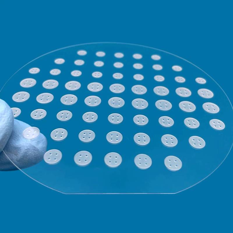
For glass wafer substrates and TGV interposers, achieving micro-crack-free dicing with low kerf width and near-zero taper angle is a requirement for advanced packaging. Traditional blade and nanosecond laser dicing cannot meet these specifications without compromising yield or device performance.
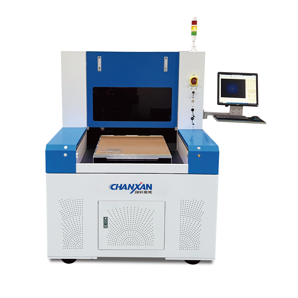
Chanxan Laser's Picosecond Laser Wafer Dicing Machine is specifically engineered to meet the ultra-fine tolerances demanded by glass substrate processing, offering:
Adjustable pulse duration (5–15 ps) to optimize the ablation mechanism for different glass compositions
On-the-fly beam shaping to control ablation profile and minimize taper
Proprietary software algorithms that compensate for the variable absorption of glass substrates
Optional 532 nm wavelength for applications requiring higher absorption
Heat-affected zone of less than 3 μm, preserving the pristine glass surface necessary for subsequent TGV metallization
Whether you are dicing 300 μm glass wafers for interposers or 1 mm thick glass for MEMS packaging, our system delivers the precision and process stability required for high-volume manufacturing.
Inquire our engineers for a free sample dicing test today →
Q: Can picosecond laser dicing create through-glass vias (TGVs) in addition to dicing?
Q: How does the dicing process affect glass substrate warp and stress for panel-level packaging?
Q: Is there any post-dicing annealing required for glass wafers?
| Free solution
Previous: Laser Dicing of Compound Semiconductors (GaAs/InP): Balancing Fragility and Precision
Next: Precision Laser Dicing for GaN-on-Silicon and GaN-on-Sapphire Wafers