Key Words: Silicon Wafer Dicing PCB Depaneling Glass Cutting
Home > Products > Laser Micromachining Systems
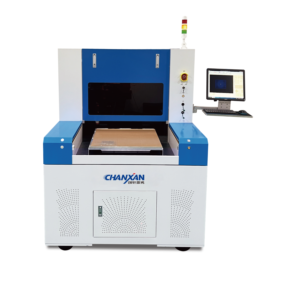

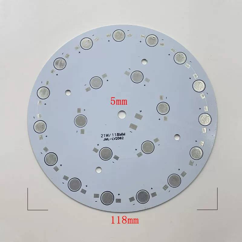

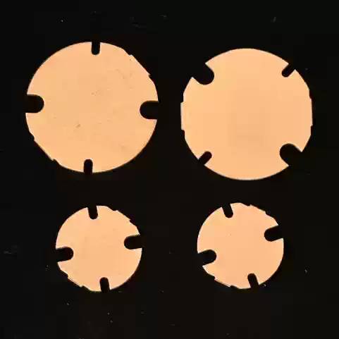


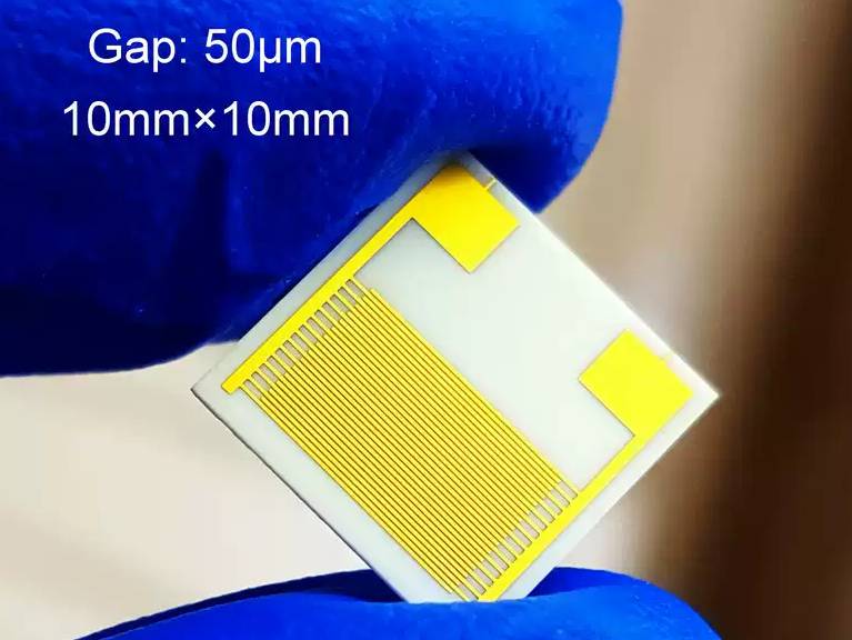
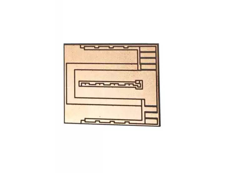
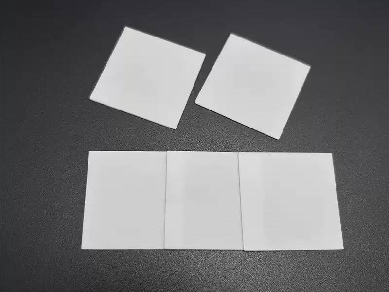

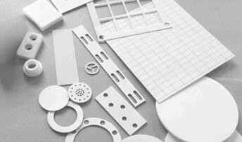
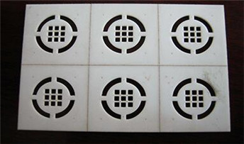
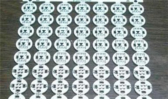
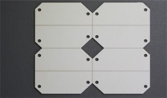
Alumina Ceramic, Aluminum Nitride Ceramic, Silicon Nitride Ceramic, High-precision cutting, drilling, and micro-structuring
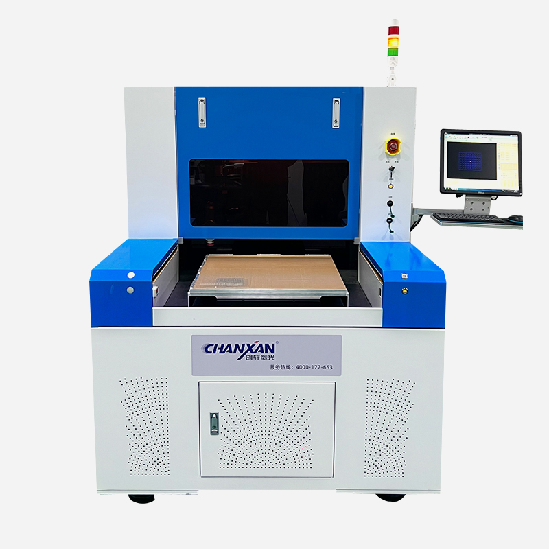
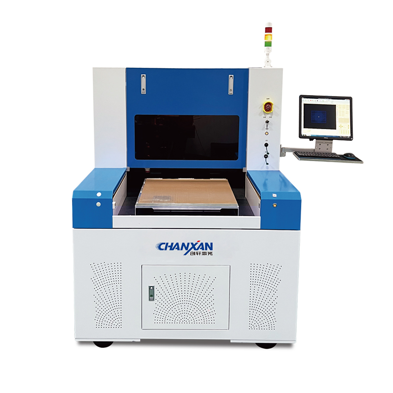
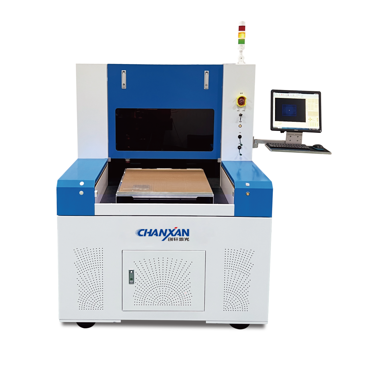
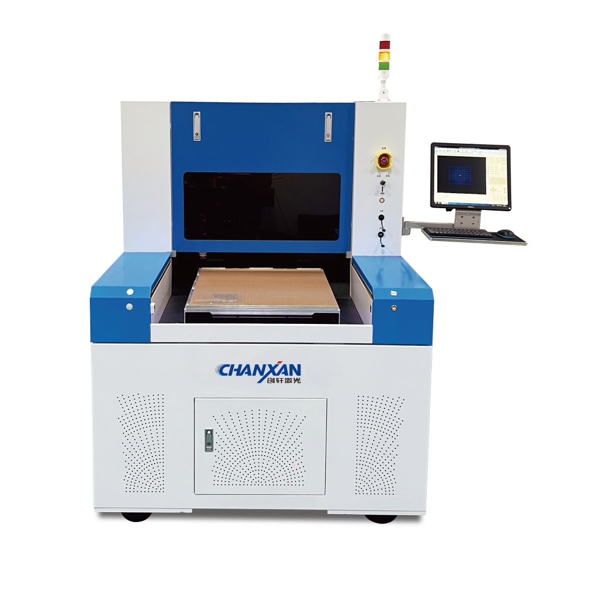
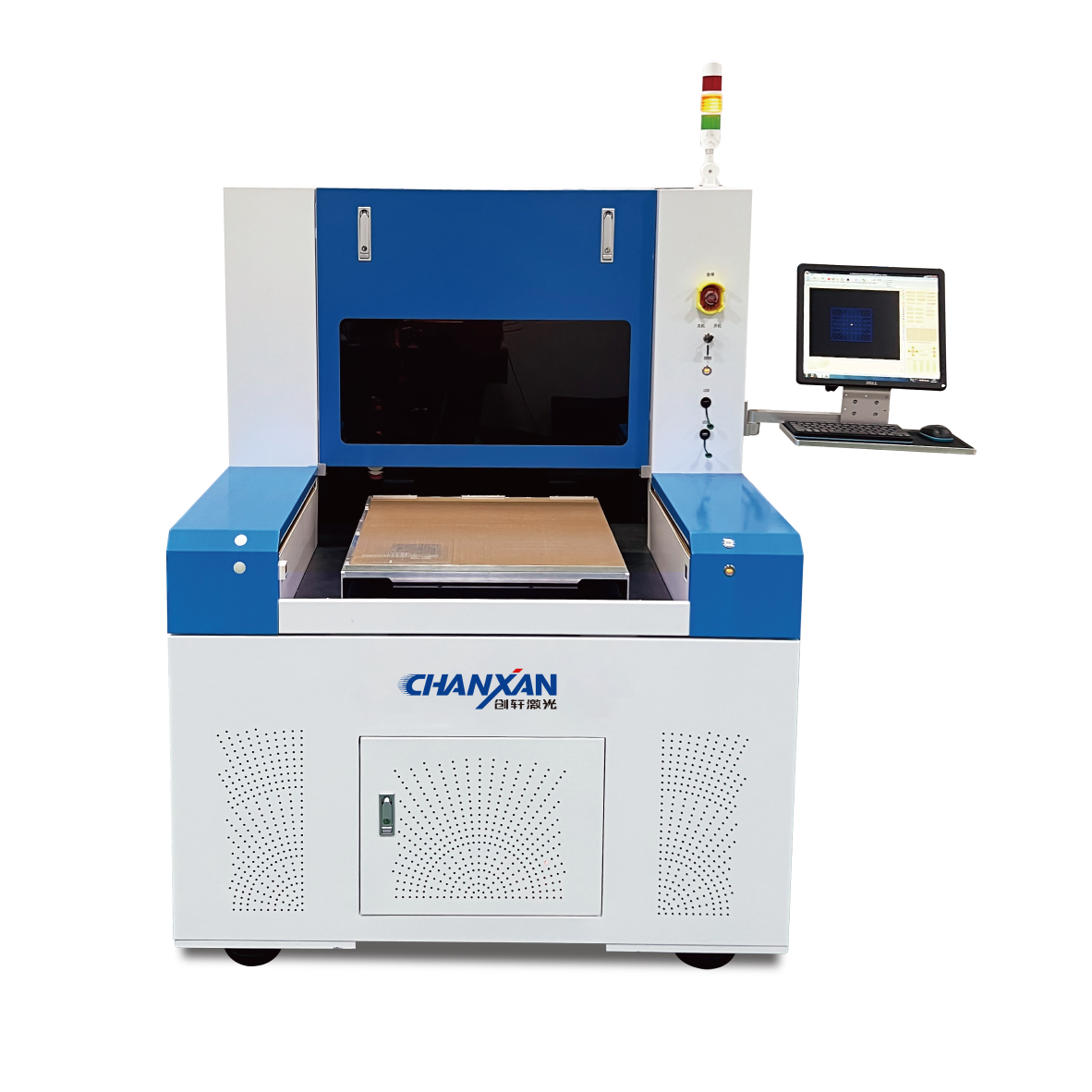
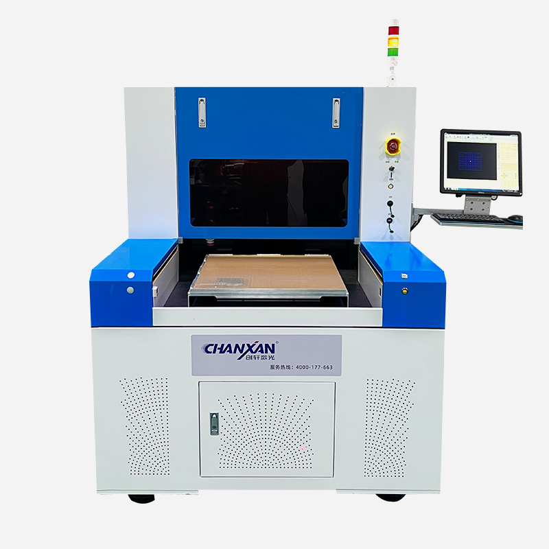
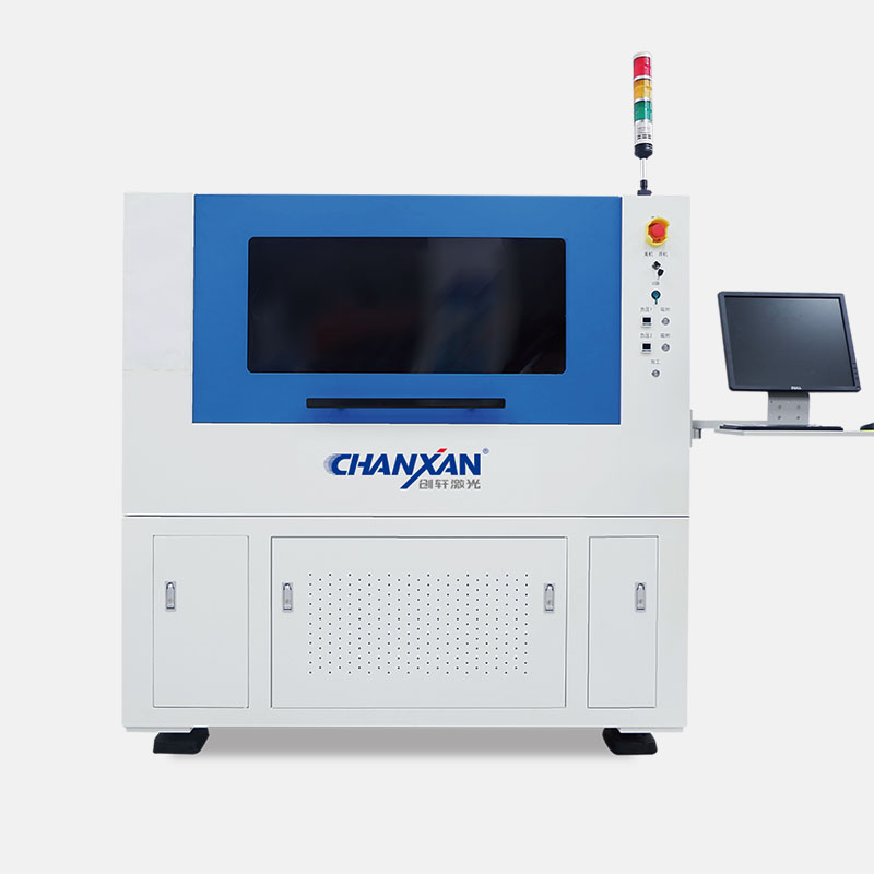
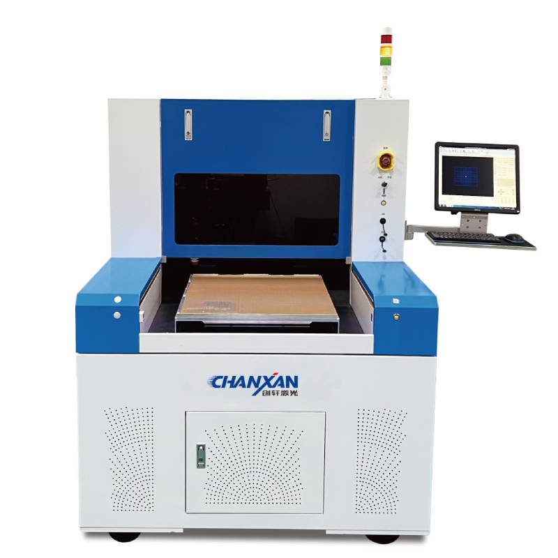
The Chanxan ceramic substrate laser cutting machine is specifically engineered for precision processing of ceramic substrates used in power electronics and semiconductor packaging, including Al₂O₃, AlN, and Si₃N₄ materials. This platform utilizes ultraviolet picosecond laser cutting technology, which has superior microcrack control, edge integrity and thermal stress management capabilities, making it suitable for laser cutting of ceramic substrates.
Ceramic substrates are widely used in high-power electronic systems due to their excellent thermal conductivity, electrical insulation, and mechanical stability. However, their inherent brittleness makes them extremely sensitive to mechanical stress and thermal shock during processing. The Chanxan ceramic substrate laser cutting machine uses picosecond ultrafast laser pulses to achieve non-contact cold ablation, eliminating mechanical force and minimizing heat affected zone (HAZ). This ensures stable processing of Al₂O₃ ceramic substrate, AlN ceramic substrate, and Si₃N₄ ceramic boards without inducing microcracks or edge chipping.
Edge chipping and surface damage
Subsurface microcracks from mechanical stress
Thermal stress accumulation in the material
Delamination in multilayer ceramic structures
Reduced long-term reliability and stability
Non-thermal ablation removes material without heat damage
Ultrashort energy pulses minimize heat affected zone
Crack-free edges with superior edge quality
No mechanical force applied to brittle materials
Ideal for high-reliability ceramic substrate applications
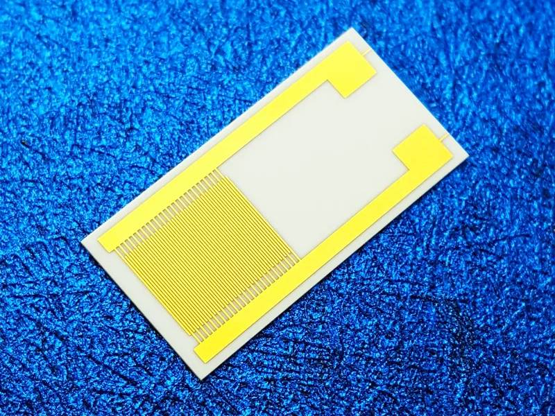
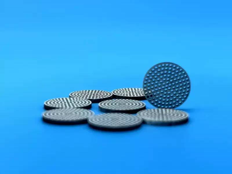
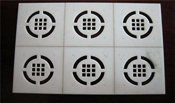
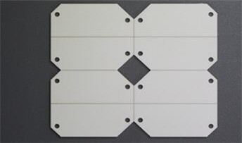
High-quality ceramic substrate processing results showing crack-free edges, no chipping, no thermal discoloration, and stable micro-geometry accuracy.
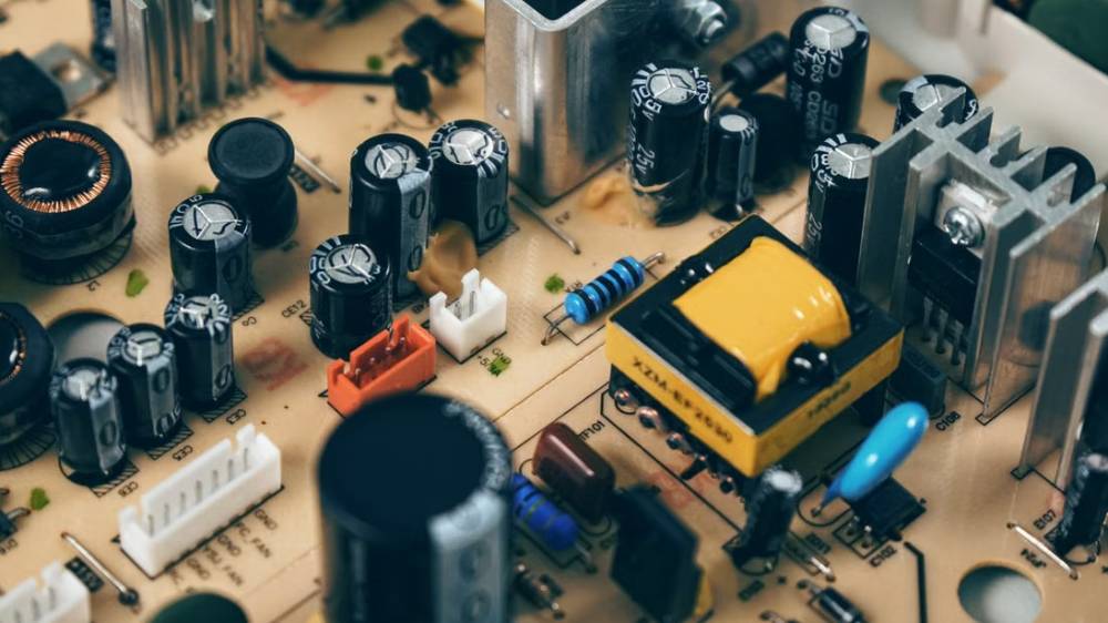
Used for ceramic substrate cutting in IGBT modules, SiC power devices, and high-voltage converters. Ensures high insulation reliability and thermal stability in power systems.
IGBT modules
SiC power devices
High-voltage converters
Power module substrates

Applied in inverter ceramic substrates, OBC modules, DC-DC converter ceramic boards, and battery power control systems. Ceramic substrates ensure stable operation under high temperature and vibration environments.
Inverter ceramic substrates
OBC (On-board charger) modules
DC-DC converter ceramic boards
Battery power control systems
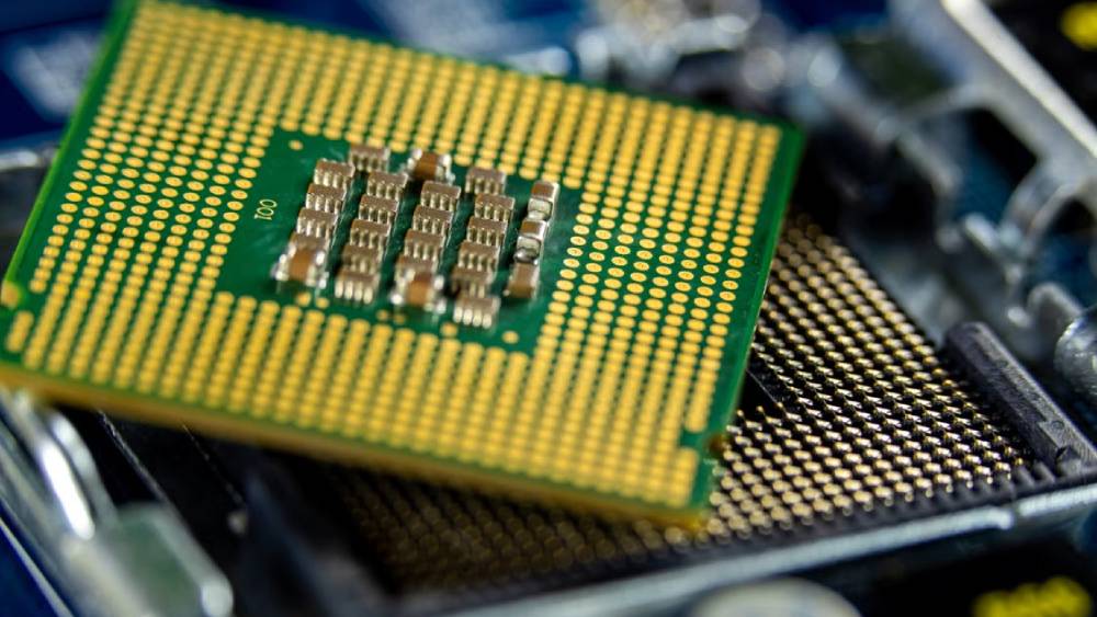
Used for ceramic substrate micro-machining in advanced packaging structures, including high-power chip modules, thermal dissipation substrates, and multi-layer ceramic interconnect structures.
High-power chip modules
Thermal dissipation substrates
Multi-layer ceramic interconnect structures
Advanced packaging applications
Supports ceramic substrate processing for 5G RF modules, high-frequency circuit substrates, and microwave power devices. Enables low-loss and high-stability signal transmission.
5G RF modules
High-frequency circuit substrates
Microwave power devices
Signal transmission systems
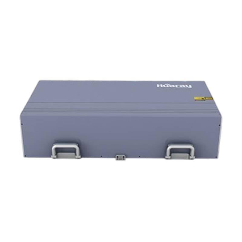
Ultrafast picosecond laser source delivering 30W power for non-thermal ablation of ceramic materials with minimal heat affected zone.
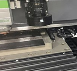
High-precision motion system with ±1μm positioning accuracy and repeatability for micron-level ceramic substrate structuring and pattern generation.
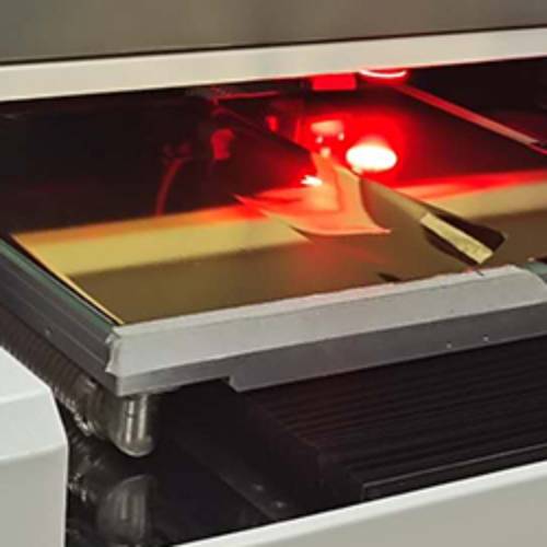
Advanced vision system for real-time substrate positioning and quality monitoring, ensuring consistent processing results and edge quality verification.
Eliminates mechanical force and thermal stress, ensuring no microcracks or edge chipping in brittle ceramic materials.
Picosecond pulses provide ultrashort energy delivery with minimal thermal damage to surrounding material.
Achieves ≤30μm accuracy with ±1μm positioning for complex ceramic substrate geometries and fine feature cutting.
Integrated control system with advanced algorithms for optimal laser parameters and motion coordination.
Multiple configuration options: 500×500mm or 600×900mm working area to accommodate various ceramic substrate sizes.
Designed for production environments with consistent processing quality and long-term operational stability.
| Feature | Specification |
|---|---|
| Model | CW-6050PZ |
| Laser Type | Picosecond UV / Green / IR |
| Laser Power | 30W |
| Working Area | 500 × 500mm / 600 × 900mm |
| Max Thickness | ≤3mm ceramic substrate |
| Cutting Speed | ≤3000mm/s |
| Positioning Accuracy | ±1μm |
| Repeatability | ±1μm |
| Overall Accuracy | ≤30μm |
| Motion System | X/Y/Z linear motor platform |
| Control System | Chanxan self-developed software |
| Supported Files | DXF, DWG, AI, PLT, BMP, etc. |
| Voltage | 380V ±10%, 50Hz |
Empowering global manufacturing with 14+ years of expertise, dual CE & ISO certified quality, over 100 national patents, and a comprehensive Technical Training Service designed for your operational success.
Systematic Training: Comprehensive full-process skill coverage.
Expert Support: Continuous project follow-up by senior engineers.
Multiple Formats: Flexible learning modes to maximize operational efficiency.
Outcome Driven: Empowering clients from "knowing" to "mastering" technology.
24H Fast Response: Technical diagnosis and solutions within 24 hours.
Warranty Policy: 1-year machine warranty with lifetime technical support.
Global Parts Supply: Rapid delivery of original parts via global network.
Lifecycle Care: From installation to long-term maintenance and software upgrades.
In-depth analysis of your specific material and performance requirements.
Precision laser sampling to verify the feasibility of the technical solution.
Bespoke manufacturing under ISO9001 quality management systems.
Final testing, professional wooden packing, and secure global shipment.
We are seeking professional partners to expand our presence in the global industrial laser market. Scale your business with Chanxan's high-end technology and manufacturing strength.
Become an AgentApplications
Subscriber:Ceramic Substrate Laser Drilling Machine