

Key Words: Silicon Wafer Dicing PCB Depaneling Glass Cutting
Home > News > Industry News
【Description】:
A comprehensive technical comparison between 355nm UV nanosecond and picosecond lasers for LTCC green tape via drilling.
In fabricating multilayer LTCC (Low‑Temperature Co‑fired Ceramic) substrates, drilling is one of the most critical steps determining electrical yield, mechanical reliability, and production cost. As via diameters shrink below 100 μm and layer counts rise, the choice of laser source becomes a strategic decision. Among UV laser solutions, two pulse-duration regimes dominate the discussion: nanosecond (10–50 ns) and picosecond (10 ps). Both operate at the 355 nm wavelength—ideal for green tape processing due to strong absorption by organic binders—but their physical interaction mechanisms with the material differ fundamentally, leading to distinct trade‑offs in quality, speed, and cost.
When a nanosecond UV pulse strikes the green tape, the organic binder and ceramic particles absorb the photon energy. The pulse duration (typically 10–50 ns) is long enough for thermal diffusion to occur within the material. The absorbed energy heats the affected volume, causing the organic components to decompose and the ceramic to fracture through thermal stresses. Material removal occurs primarily through melting, vaporisation, and mechanical ejection of molten or softened material.
This thermal nature has two consequences:
A heat‑affected zone (HAZ) extends beyond the drilled hole, where the binder may be partially degraded or the ceramic structure altered.
Molten debris and recast layers may form on the hole walls and surrounding surface.
However, nanosecond lasers offer a key advantage: high single‑pulse energy (typically 50–200 μJ or more), enabling efficient material removal per pulse. This translates directly to higher drilling speeds for a given average power.
With picosecond pulses (10 ps), the energy is deposited into the material faster than the thermal diffusion time (which is on the order of nanoseconds for typical ceramics and polymers). The material transitions directly from solid to vapour through sublimation or plasma‑mediated ablation—a process often described as "cold ablation." Because heat has no time to diffuse into the surrounding material, the HAZ is dramatically reduced, and the ejected material is largely gaseous, leaving minimal molten debris.
The trade‑off: picosecond lasers deliver lower single‑pulse energy (typically 10–50 μJ) at the same average power. More pulses are required to remove the same volume of material, which can reduce drilling throughput if not compensated by higher repetition rates or optimised scanning strategies.
Typical HAZ: 10–20 μm (measured from the via edge).
At optimised parameters (e.g., 200 kHz, 1000 mm/s, 15 μJ), the HAZ can be limited to 8–12 μm.
Visible under optical microscopy as a darkened ring surrounding the via (binder burn‑out & partial sintering).
Typical HAZ: <5 μm, often 1–3 μm.
Under high‑magnification SEM, transition from drilled edge to unaffected tape is abrupt without visible thermal damage.
Eliminates the darkened ring entirely, preserving original properties up to the via edge.
For applications where HAZ must be minimised—such as high‑frequency RF substrates where dielectric loss is critical, or thin tapes (<75 μm) where thermal damage can cause handling failures—picosecond lasers offer a decisive advantage. For standard LTCC applications where a 10–20 μm HAZ is acceptable, nanosecond lasers provide sufficient quality at lower cost.
Debris generated during via drilling can contaminate the green tape surface, interfere with subsequent lamination, and cause via filling defects. Recast material on the hole walls can increase via resistance and reduce metallisation adhesion.
Debris: Molten droplets eject and deposit on surrounding surface (extends 50–100 μm).
Recast layer: A thin (1–3 μm) re‑solidified layer on hole walls.
Mitigation: Gas assist reduces debris but cannot eliminate it entirely.
Debris: Material ejection is gaseous; fine particulate easily cleaned.
Recast layer: Essentially absent; clean hole walls with original tape texture.
Mitigation: Standard extraction keeps the surface exceptionally clean.
Picosecond lasers produce significantly cleaner vias and surfaces, reducing the need for post‑drilling cleaning steps. This is particularly important for high‑density designs where debris can bridge adjacent vias or interfere with fine conductor patterns.
Via edge quality affects both electrical performance (via resistance, impedance control) and mechanical reliability (crack initiation).
Taper: 5–15° taper from entry to exit depending on focus/energy.
Roundness: Deviation is <5 μm for 100 μm vias.
Micro‑cracks: Thermal stress may induce micro-cracks in ceramic matrix.
Taper: Minimal taper (<5°), producing nearly vertical hole walls.
Roundness: Deviation <3 μm, enabling tighter via pitch.
Micro‑cracks: Cold ablation avoids thermal stress, eliminating cracks completely.
Picosecond lasers deliver superior edge quality—straighter walls, tighter roundness, and no micro‑cracks. For high‑reliability or high‑density designs, this quality advantage justifies the higher equipment cost.
The choice between UV nanosecond and picosecond lasers for LTCC green tape micromachining is not a simple "one is better" decision—it depends on the specific requirements of the application, the acceptable trade‑offs between quality and throughput, and the total cost of ownership.
Chanxan Laser offers both nanosecond and picosecond UV laser systems, purpose‑built for LTCC green tape via drilling. Our application engineers work with customers to determine the optimal pulse duration for their specific tape formulation, via size, layer count, and production volume.
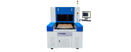
UV Nanosecond Systems: For high‑throughput production of standard vias (75 μm), delivering excellent cost‑per‑via and proven reliability.
UV Picosecond Systems: For high‑precision, high‑reliability applications requiring via diameters below 50 μm, minimal HAZ (<5 μm), and micro‑crack‑free edges.
Process Development Support: Chanxan's application laboratory provides sample drilling trials, parameter optimisation, and comprehensive characterisation (SEM, HAZ measurement, via resistance) to ensure that your process meets the most demanding specifications.
Global Service Network: With rapid response and genuine spare parts, Chanxan ensures that your production line remains operational and efficient.
Contact our laser micro-machining specialists today to discuss your LTCC green tape processing requirements or request a free sample drilling trial.
Contact Chanxan Laser| Free solution
Previous: High‑Aspect‑Ratio LTCC Via Drilling: Laser Process Optimisation Guide
Next: Laser Drilling vs. Mechanical Punching for LTCC Green Tapes: A Head‑to‑Head Comparison








