Key Words: Silicon Wafer Dicing PCB Depaneling Glass Cutting
Home > News > Industry News
【Description】:
Achieve crack-free cutting and dense via drilling for advanced ceramics. High-precision laser solutions for Alumina, AlN, Zirconia & LTCC/HTCC substrates.
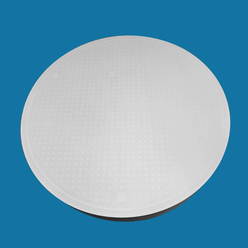
Alumina, aluminum nitride, zirconia, silicon nitride and LTCC/HTCC substrates power the electronics, medical and energy industries — and their hardness and thermal sensitivity make conventional machining slow, chip-prone, and hard to hold to tolerance.
Alumina and zirconia wear through mechanical tooling quickly, driving up tool cost and introducing inconsistent edge quality as tools degrade mid-run.
Aluminum nitride and silicon nitride conduct and store heat differently across their structure, so uneven heat input during processing can trigger microcracking or delamination.
Electronic substrates and LTCC/HTCC packages call for via arrays and slots at scales where mechanical drilling and dicing saws struggle to hold position and avoid chipping.
Multilayer ceramic packages combine conductive and dielectric layers with different responses to heat and mechanical stress, so a process tuned for one layer can damage the next.
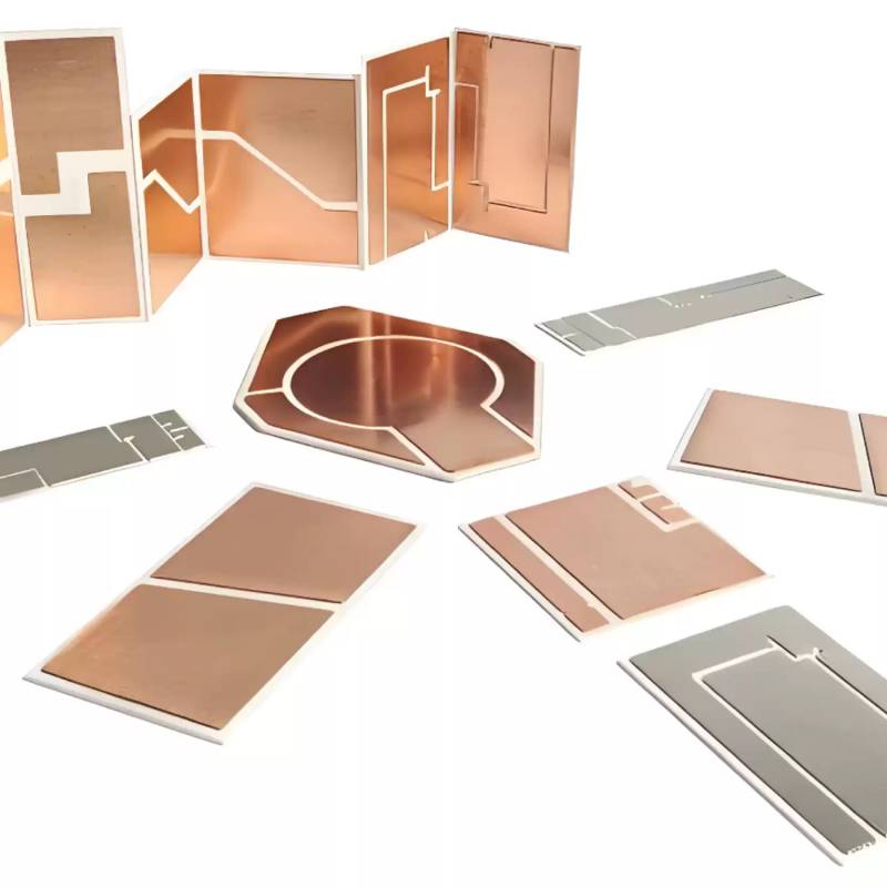
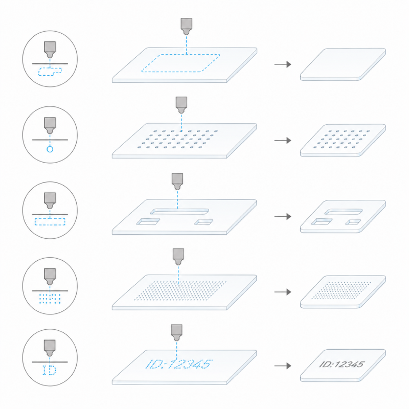
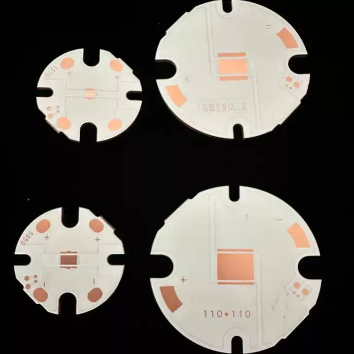
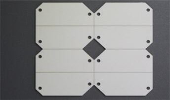
Substrates and green-state or sintered ceramic sheets are cut to outline with controlled heat input, keeping edge chipping and micro-fracture within tight limits.
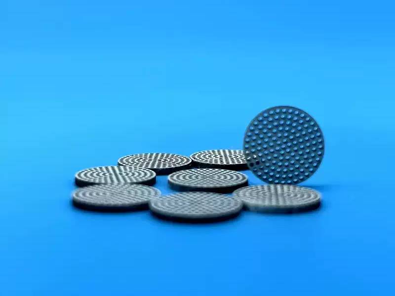
Dense via arrays for electrical interconnects are drilled at fine pitch with consistent hole taper, supporting high-density substrate and package designs.
Slots and cavities for component mounting or thermal relief are machined without inducing the stress concentrations that lead to later-stage cracking.
Controlled texturing improves adhesion for metallization or bonding layers on power electronics and substrate surfaces.
Permanent identification and traceability codes are marked directly on the ceramic surface without affecting mechanical or electrical performance.
Microscopic processing results showing clean edges, zero delamination, and precise via geometry.
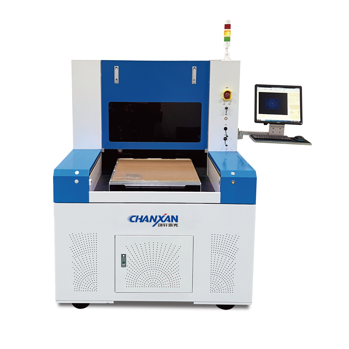
These are the industry segments where Chanxan laser systems are deployed for advanced ceramics processing.
| Free solution