Key Words: Silicon Wafer Dicing PCB Depaneling Glass Cutting
Home > News > Industry News
【Description】:
Industrial laser equipment for Fused Silica, BK7 & Lithium Niobate processing. Build turnkey systems to eliminate subsurface damage & wavefront distortion.
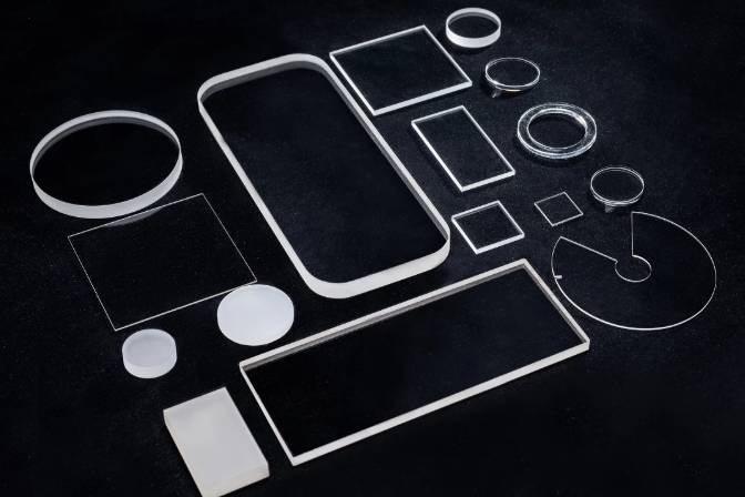
Fused silica, BK7 glass, lithium niobate and infrared crystals carry the light in laser, photonic and imaging systems — and any subsurface damage or roughness introduced during processing shows up directly as optical loss or wavefront error.
Fused silica and BK7 glass reveal even microscopic subsurface damage as scatter loss or reduced laser damage threshold in the finished optic.
Lithium niobate and other nonlinear crystals respond differently to processing depending on crystal axis, requiring orientation-aware parameter control.
Photonic chips and microfluidic optics need internal channels and structures at scales where conventional machining cannot reach without breaking the part.
Infrared crystals used in thermal imaging must keep transmission uniform across the aperture, so edge and surface damage from processing directly limits system performance.
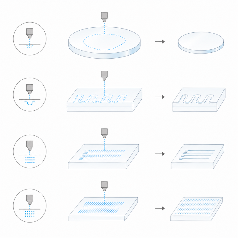
Precision cold cutting separates optical blanks along the target contour while preserving edge strength and minimizing subsurface damage depth.
Internal microchannels for photonic and microfluidic devices are formed with controlled wall smoothness and dimensional accuracy.
Fine surface and volume structures — including waveguide features and diffractive elements — are machined to sub-micron positional accuracy.
Functional surface patterns for anti-reflection, diffusion, or coupling are applied without introducing scatter-inducing surface defects.
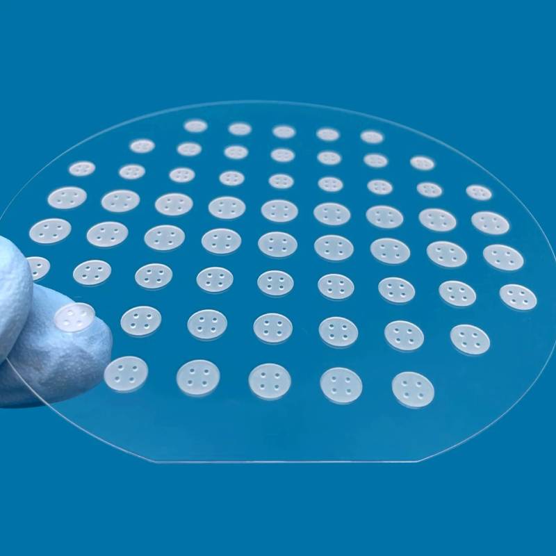
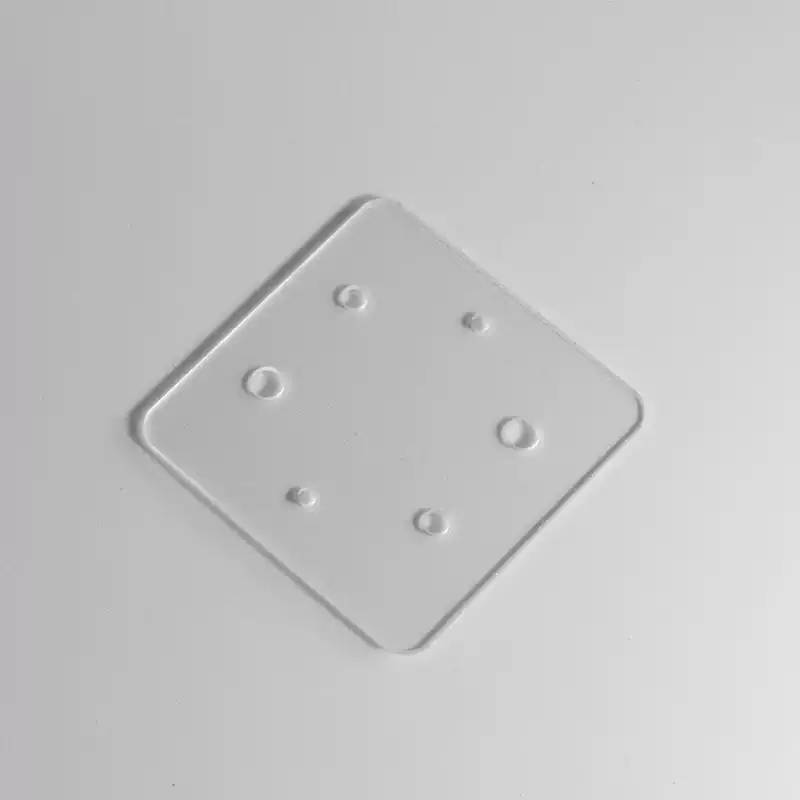
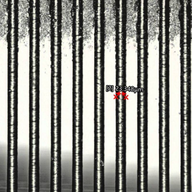
Microscopic processing results showing clean edges, low subsurface damage, and precise micro-feature control.
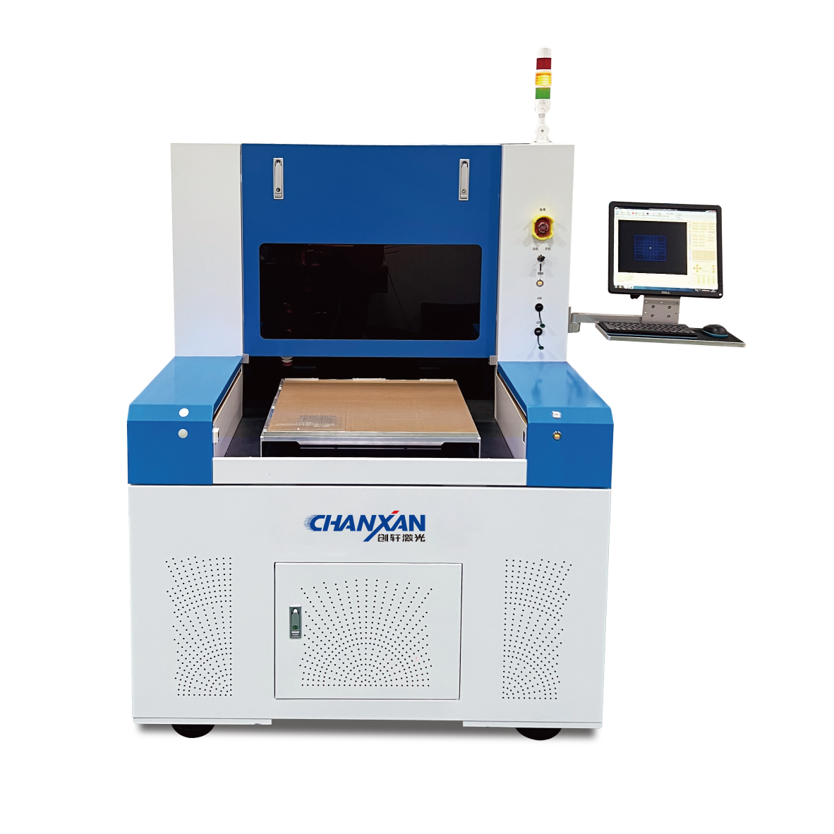
These are the industry segments where Chanxan laser systems are deployed for optical and photonic material processing.
| Free solution