Key Words: Silicon Wafer Dicing PCB Depaneling Glass Cutting
Home > News > Industry News
【Description】:
Boost die yield with Chanxan high-precision wafer laser dicing solutions. Zero-chipping cutting, grooving & micro-drilling for silicon, SiC, GaN & glass wafers.
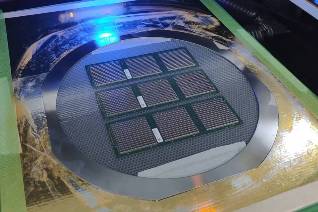
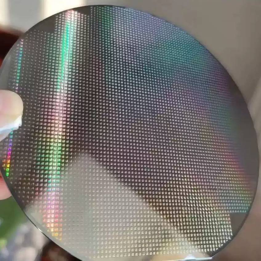
Silicon, SiC, GaN, glass and compound semiconductor wafers carry increasingly dense, increasingly thin die — and every micron of chipping or heat-affected zone at the street eats directly into device yield.
Mechanical saw dicing generates edge chipping that directly reduces die strength and shrinks usable die area as device geometries continue to shrink.
Thinned wafers for advanced packaging flex and crack under saw-induced mechanical stress, making non-contact separation increasingly necessary at scale.
SiC and GaN wafers are harder and more brittle than silicon, wearing down saw blades quickly and driving up consumable cost and downtime.
Narrower dicing streets on modern layouts leave less margin for kerf width and heat-affected zone, raising the bar for cut precision.
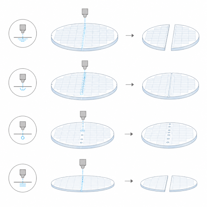
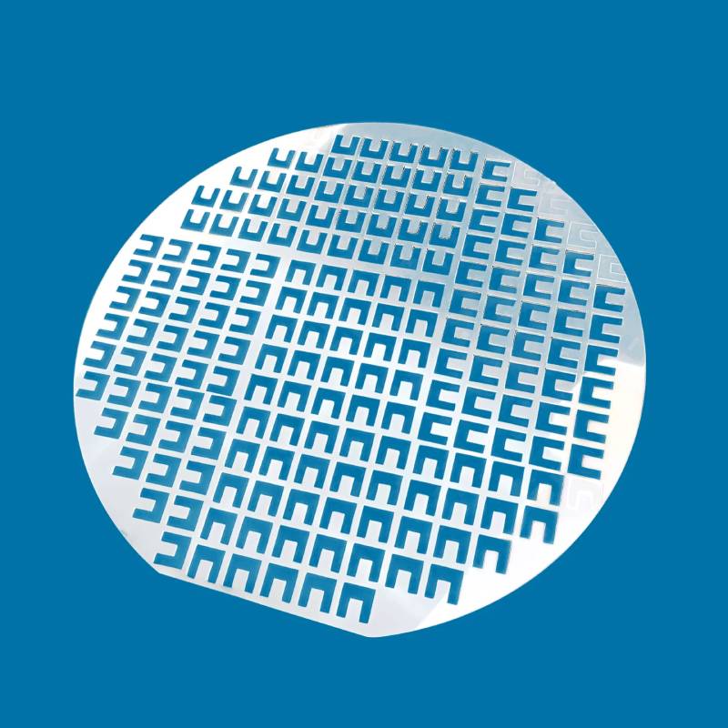
Full-thickness ablation dicing separates die along the street with narrow kerf width and minimal chipping at the top and bottom surface.
Shallow grooves cut through passivation and metal layers ahead of mechanical or stealth separation, protecting the underlying die from chipping.
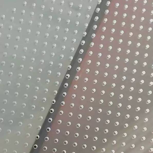
Fine through-silicon vias and alignment features are formed with controlled hole taper for advanced packaging and MEMS structures.
Sub-100 micron wafers used in advanced packaging are cut without the mechanical load that would otherwise crack or warp the thinned substrate.
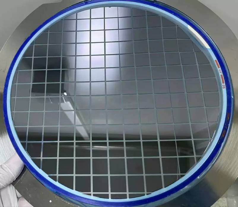
Microscopic processing results showing narrow kerf, zero chipping, and consistent die separation.
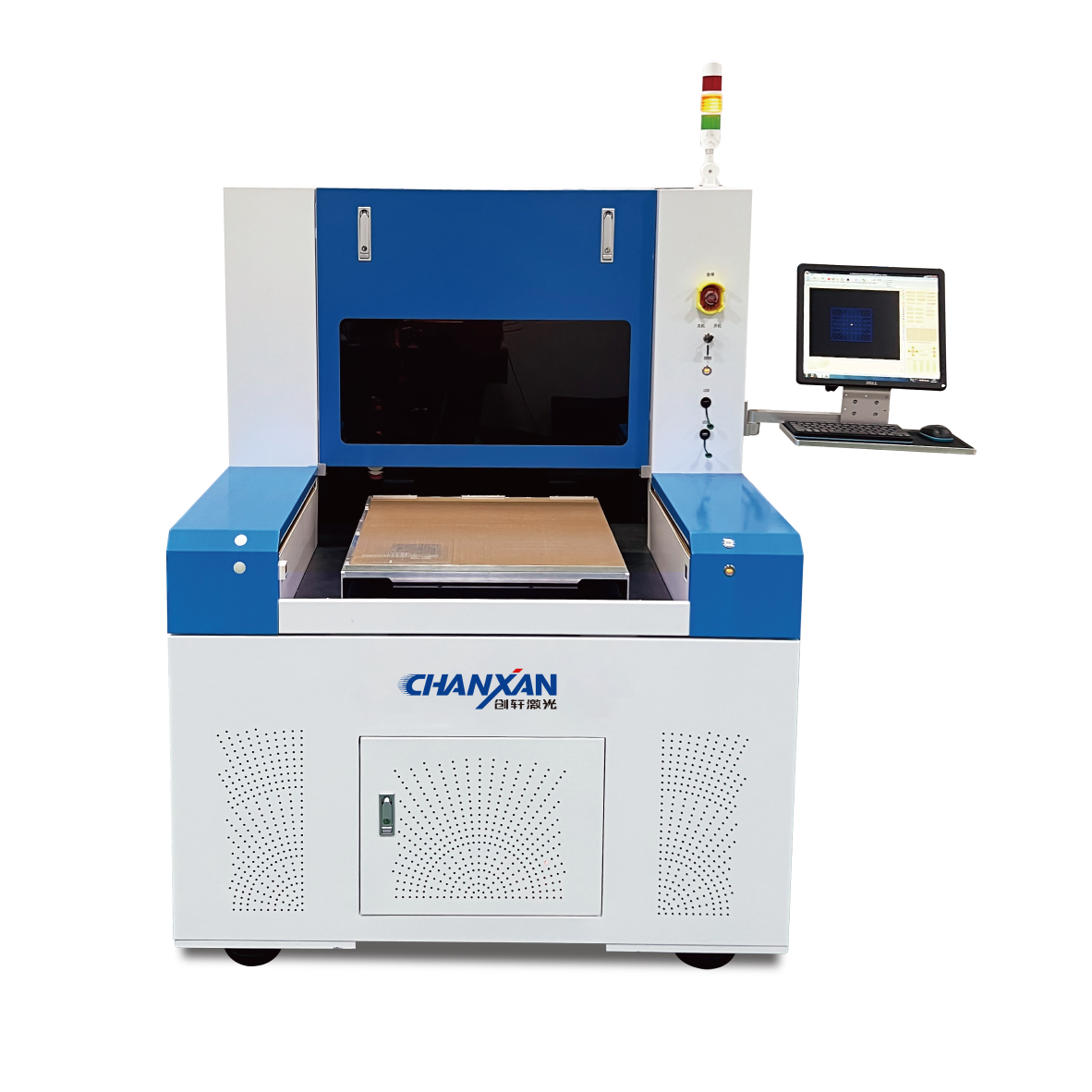
These are the industry segments where Chanxan laser systems are deployed for semiconductor wafer processing.
| Free solution
Previous: Optical & Photonic Laser Processing
Next: Laser Processing for Solid-State Battery & New Energy Materials