

Key Words: Silicon Wafer Dicing PCB Depaneling Glass Cutting
Home > News > Industry News
【Description】:
Discover high-precision fused silica laser cutting and micromachining solutions. Learn how ultrafast lasers eliminate edge chipping and subsurface damage in optical glass manufacturing.
In the realm of advanced optics, photonics, and semiconductor manufacturing, fused silica stands out as a critical substrate. Its exceptional material characteristics make it indispensable, yet these same properties present significant engineering challenges during fabrication. Traditional mechanical machining methods often fall short, struggling to meet the tight tolerances and pristine edge quality required for next-generation applications.
To overcome these limitations, high-precision fused silica laser cutting and fused silica micromachining have emerged as the industry standards. By leveraging advanced laser technologies, manufacturers can achieve unprecedented accuracy, intricate geometries, and damage-free edges.
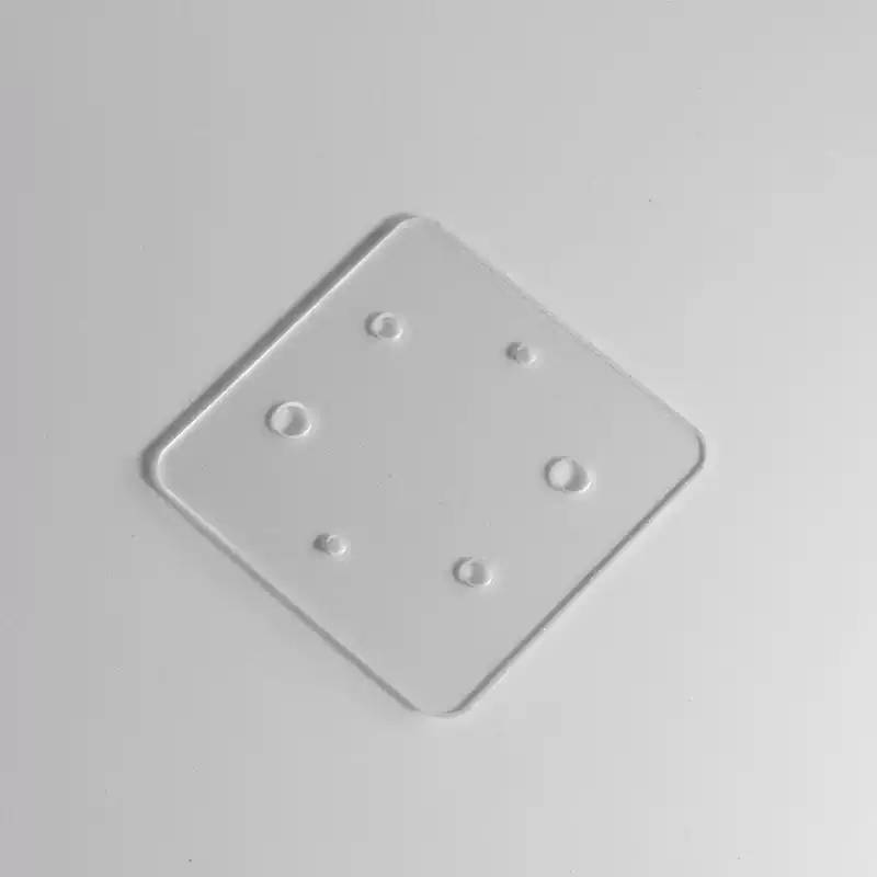
Fused silica is a synthetic, high-purity amorphous silicon dioxide (SiO₂) glass. Unlike standard soda-lime or borosilicate glasses, it is manufactured using vapor-phase oxidation of silicon tetrachloride, resulting in an incredibly pure material with unique physical attributes:
Low Thermal Expansion: Fused silica features a remarkably low coefficient of thermal expansion (≈ 0.5 x 10⁻⁶/K). This provides extraordinary thermal shock resistance, allowing optical components to maintain dimensional stability under extreme temperature fluctuations.
High UV Transmission: It offers an exceptionally broad optical transmission spectrum, extending from deep ultraviolet (DUV) through the visible spectrum and into the near-infrared (NIR) wavelengths.
High Laser Damage Threshold (LDT): Its high purity gives it a superior resistance to intense optical radiation, making it the preferred substrate for high-power laser optics and beam-delivery systems.
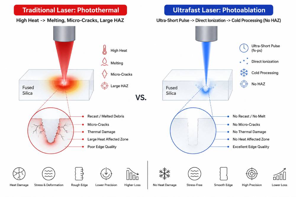
To bypass the pitfalls of mechanical and thermal stress, the industry has shifted toward ultrafast laser fused silica processing. By using pulse widths in the picosecond or femtosecond regime, the physics of the material interaction changes fundamentally.
Extreme Brittleness: Amorphous structure is highly susceptible to mechanical stress.
Edge Chipping: Contact causes micro-chipping at entry/exit points.
Subsurface Damage (SSD): Micro-cracks propagate hidden structural defects.
Surface Roughness: Post-polishing adds high cost and distorts tolerances.
No Melting: Direct solid-to-plasma vaporization leaves zero recast layers.
Minimal HAZ: Heat-affected zone is well restricted under a few microns.
Crack Prevention: Eliminates thermal stress, protecting subsurface integrity.
Superior Edge Quality: Femtosecond laser fused silica cutting achieves mirror-smooth finishes.
When executing picosecond laser glass processing or femtosecond cutting, the laser pulse is delivered in a timeframe shorter than the material's electron-phonon coupling time (less than a few picoseconds). The peak power density is so high that electrons are instantly excited via multi-photon absorption, ripping the atomic bonds apart before thermal energy can conduct into the surrounding lattice.
Modern laser cutting fused silica platforms are highly versatile, capable of performing multiple high-precision geometries on a single system:
Precision Cutting: Dicing complex outer profiles, internal cutouts, and slots in wafers or optical plates without fracturing.
High-Aspect-Ratio Drilling: Creating micro-vias and tapered holes with diameters down to tens of micrometers.
Microchannels & Microfluidics: Scribing precise subsurface or surface channels for lab-on-a-chip devices.
Surface Texturing: Modifying topography at the micron scale to alter optical reflectivity or adhesion.
Waveguide Preparation: Writing highly localized refractive index changes inside the bulk glass for photonic circuits.
The capabilities of advanced fused silica laser machining support a wide array of high-tech industries:
Optical Windows & Beam Splitters: For high-power industrial lasers, aerospace sensors, and deep-UV lithography.
Microfluidics: Complex glass chips used in chemical synthesis, DNA sequencing, and biomedical research.
Laser Optics: High-damage-threshold lenses, mirrors, and prisms used in scientific laser systems.
Photonic Devices: Optical interconnections, fiber-optic couplers, and arrayed waveguide gratings (AWGs).
Achieving flawless results requires a perfect synergy between motion control, beam delivery, and laser source dynamics.
| Free solution
Previous: BK7 Glass Laser Cutting and Micromachining for Precision Optical Manufacturing
Next: Precision Laser Drilling & Scribing for LTCC/HTCC Multi‑layer Ceramic Substrates








