Key Words: Silicon Wafer Dicing PCB Depaneling Glass Cutting
Home > News > Industry News
【Description】:
High-precision UV & picosecond laser systems for LTCC and HTCC ceramic substrates. Optimize via drilling, cutting, and slotting with zero tool wear.
LTCC (Low-Temperature Co-fired Ceramic) and HTCC (High-Temperature Co-fired Ceramic) represent the most sophisticated class of ceramic packaging technologies, enabling the 3D integration of passive and active components in a single monolithic substrate. They are the backbone of:
RF and microwave modules for 5G/6G, radar, and satellite communications.
Medical implantable devices – high-reliability hermetic packages.
Automotive ECU – compact, high-density interconnects.
MEMS and sensor packaging – embedded cavities and vias.
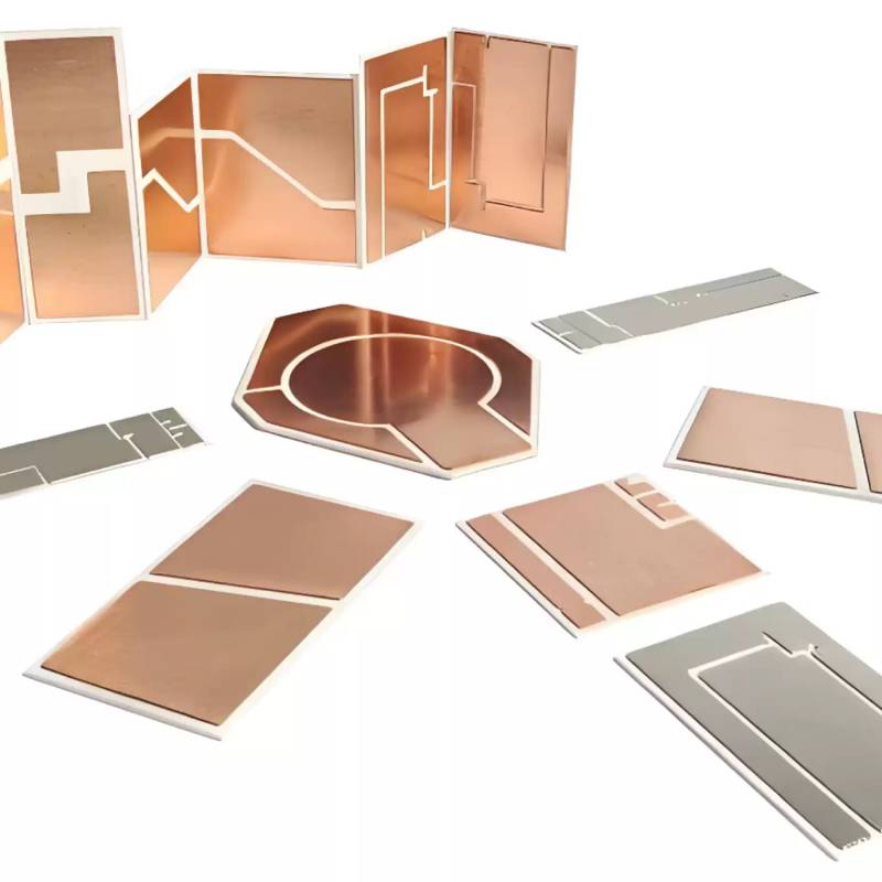
The Manufacturing Bottleneck: The production of LTCC/HTCC involves multiple steps: tape casting, via punching (mechanical or laser), screen printing of conductors, stacking, lamination, and co-firing. Via drilling and green-tape cutting are the most critical for yield and electrical performance.
Traditional mechanical punching of vias (using hard-metal punches) faces severe limitations:
Tool wear – punches wear out after 5,000–20,000 hits, leading to burrs, micro-cracks, and positional misalignment.
Limited aspect ratio – mechanical punching cannot produce micro-vias with a diameter < 100 μm reliably.
Registration errors – in multi-layer stacking, any minor misalignment of vias between layers causes complete electrical opens or shorts.
Post-firing shrinkage – the green tape shrinks 10%–15% after firing, which severely exacerbates any initial dimensional misalignment.
For scribing and singulation, conventional sawing or mechanical shearing of green or fired LTCC/HTCC creates severe edge burrs, micro-delamination between multi-layers, and stress-induced cracks that propagate catastrophically during co-firing.
To overcome these bottlenecks, deploying an advanced ceramics laser processing system equipped with high-precision UV or picosecond lasers has become the premium industry standard. Optical drilling offers:
Zero tool wear – delivers perfectly consistent via quality over millions of cycles with zero replacement overheads.
Ultra-fine vias – effortlessly drills micro-vias down to 30–50 μm in green tape, and 25–40 μm on fired ceramics.
High positional accuracy – automated laser registration to fiducial marks ensures layer-to-layer alignment accuracy < 5 μm.
Flawless edges – zero mechanical stress prevents edge burrs, micro-delamination, and debris contamination.
The laser processing profile of LTCC/HTCC differs significantly depending on whether the material is processed in its green state or after final sintering:
For green tape (typically 50–200 μm thick), UV Laser (355 nm) wavelength is preferred because organic binders absorb UV energy strongly. This initiates clean photochemical decomposition with minimal heat input, leaving carbon-free via walls.
For fired LTCC/HTCC (dense glass-ceramic or alumina-based matrices), Picosecond Laser technology (355 nm or 532 nm) is deployed to ablate the hard ceramic without causing thermal shock or stress fractures.
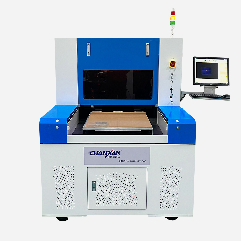
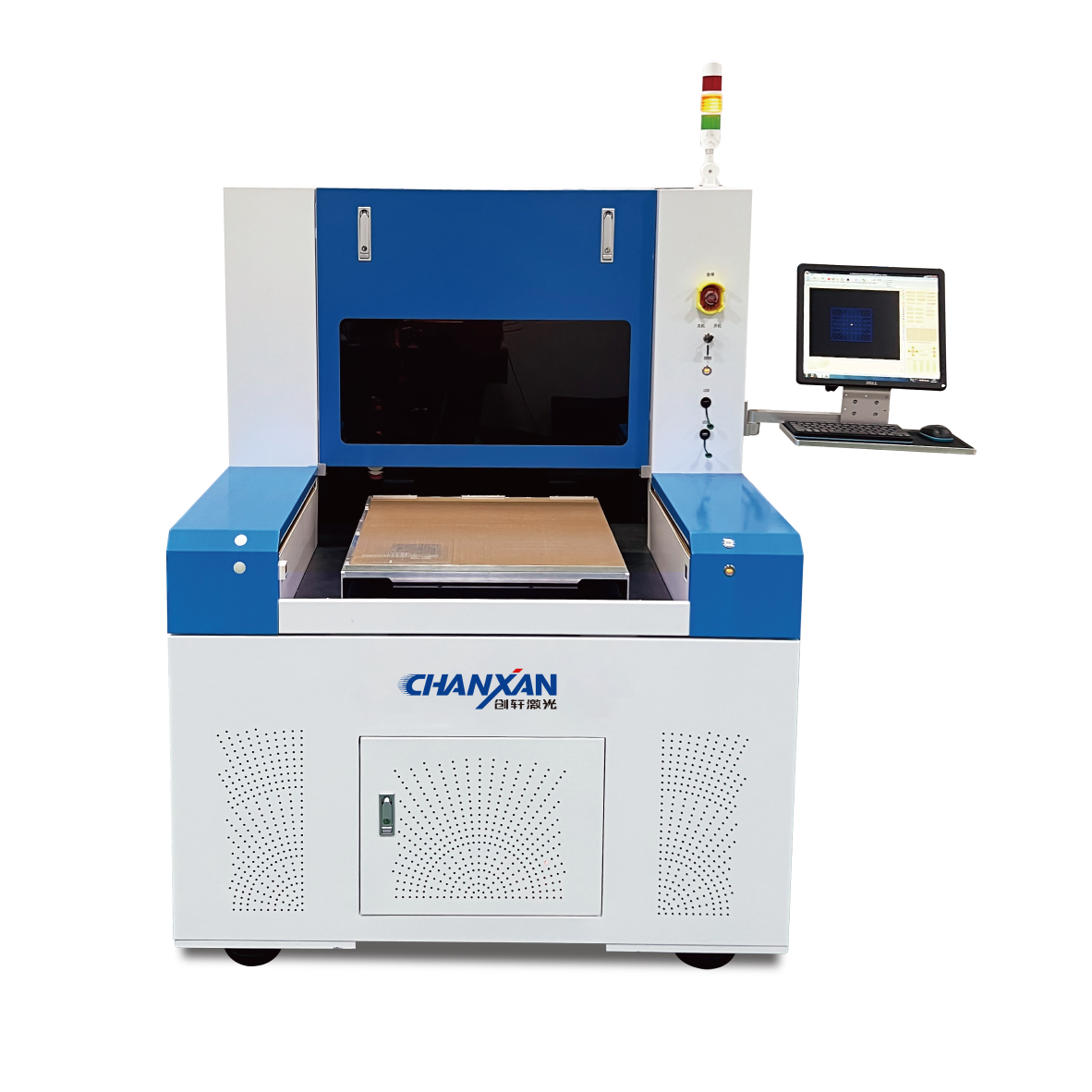
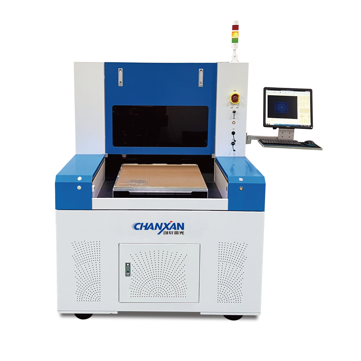
Chanxan's recommended hardware configuration for high-throughput LTCC/HTCC production integrates a UV Picosecond Laser (355 nm, 5–15 ps) with an ultra-fast galvanometer scanner and linear motor stage for rapid, micron-level via-array generation.
Our LTCC/HTCC laser micromachining systems support high-end electronic supply chains globally:
Telecommunications & RF (5G/6G, SatCom): LTCC substrates for mm-wave antenna arrays; HTCC packages for power amplifiers; via-drilled interposers.
Medical Electronics (ISO 13485): Implantable pacemaker and neurostimulator packages; hermetic sensor housings for continuous glucose monitors.
Automotive & Industrial (AEC-Q100, ISO 26262): High-temperature engine control unit (ECU) substrates; pressure sensor packages.
Defense & Aerospace: Radar transmit-receive modules and missile seeker cards with high-density multi-layer interconnections.
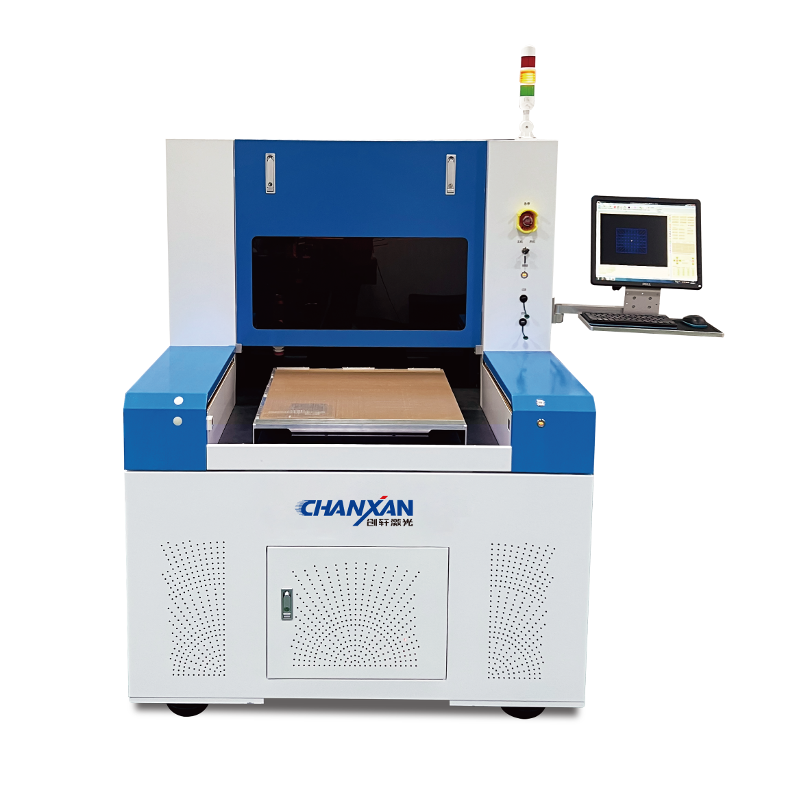
The Chanxan Picosecond Laser System is custom-engineered for high-precision, industrial-grade processing of LTCC and HTCC substrates, enabling rapid via drilling, slotting, cutting, and micro-structuring with negligible thermal impact.
| System Feature | Hardware Benefit |
|---|---|
| Ultrashort Pulse Picosecond Laser | Enables precise cold ablation with a minimized heat-affected zone (HAZ), eliminating micro-cracking, layer delamination, and thermal damage. |
| UV Laser Processing Capability | Delivers excellent material absorption and highly controlled ablation for delicate multilayer ceramic electronic substrates. |
| High-Precision Motion Platform | Features linear-driven axes to ensure superb positioning accuracy and repeatable micromachining quality for high-density via arrays. |
| Advanced Vision Alignment System | Enables automated, real-time positioning on fiducial marks, ensuring micron-level layer-to-layer registration accuracy. |
| Automatic Focus Control System | Maintains optimal focal spot size across substrate thickness variations and minor surface unevenness. |
| Efficient Fume & Debris Extraction | Instantly evacuates airborne residues to maintain cleanroom-ready processing conditions and shield sensitive optical components. |
| Flexible Process Parameter Control | Empowers engineers to easily optimize pulse overlap, scanning frequency, and laser power for both green tape and fired ceramics. |
Struggling with mechanical tool wear, micro-cracks, or layer registration errors on your co-fired ceramic layers?
Chanxan Laser Application Laboratory offers Free Hardware Feasibility Testing & Technical Sampling. Upload your CAD drawings today to receive a complete machine configuration report and optical evaluation within 48 hours.
| Free solution
Previous: Fused Silica Laser Cutting: Precision Micromachining for Optical Components
Next: Laser Machining of Silicon Nitride (Si₃N₄): High‑Speed Cutting and Drilling Solutions