Key Words: Silicon Wafer Dicing PCB Depaneling Glass Cutting
Home > News > Industry News
【Description】:
Ultrafast lasers improve wafer manufacturing through precise dicing, slicing, TSV formation, scribing, thin wafer handling, and MEMS fabrication. Picosecond and femtosecond systems reduce heat-affected zones, increase dimensional accuracy, and lower defect rates, optimizing semiconductor production.
As semiconductor device dimensions shrink and packaging processes become increasingly complex, the precision requirements for wafer fabrication have reached levels that traditional mechanical and thermal processing methods cannot meet. This guide explains what ultrafast lasers are, their applications in wafer manufacturing, and how purchasing and process engineers can evaluate which laser type best suits their production requirements.
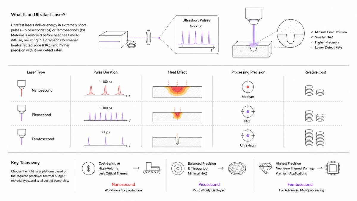
An ultrafast laser delivers energy in extremely short pulses — typically in the picosecond or femtosecond range. Unlike conventional nanosecond lasers, which deposit heat over a relatively long pulse duration, ultrafast lasers remove material before thermal energy has time to diffuse into surrounding areas. The practical result is a dramatically smaller heat-affected zone (HAZ), which translates directly to higher dimensional precision and lower defect rates in semiconductor wafers.
For procurement teams evaluating laser systems, the three key pulse regimes can be compared as follows:
| Laser Type | Pulse Duration | Heat Effect | Processing Precision | Relative Cost |
|---|---|---|---|---|
| Nanosecond | 1–100 ns | Higher HAZ | Medium | Lower |
| Picosecond | 1–100 ps | Minimal HAZ | High | Medium |
| Femtosecond | <1 ps | Near-zero thermal damage | Ultra-high | Highest |
Nanosecond lasers remain the workhorse for cost-sensitive, high-volume applications where tight thermal budgets are not critical. Picosecond lasers offer a strong balance of precision and throughput, making them the most widely deployed ultrafast type in production today. Femtosecond lasers deliver the highest precision and the cleanest material interaction, but at a capital cost that is typically justified only for premium microprocessing tasks — such as hard substrate cutting or extremely fine via formation.
Understanding this tradeoff is the first step toward selecting the right laser platform for a given semiconductor process node and material set.
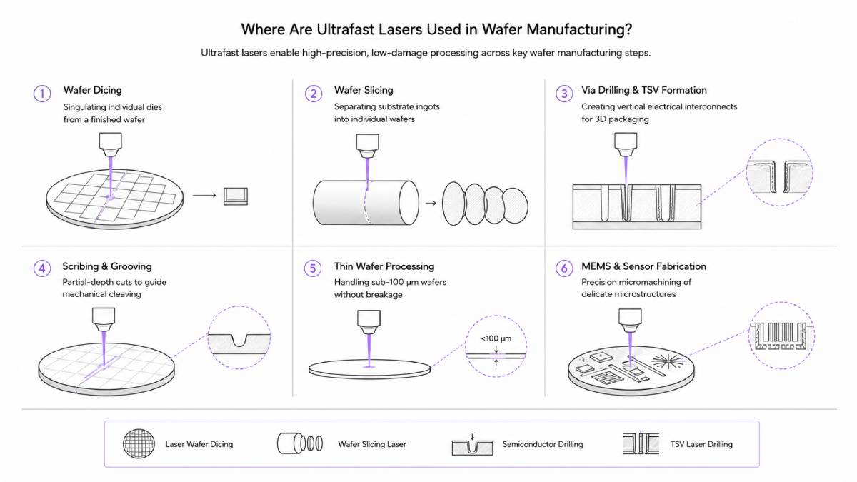
Ultrafast lasers address a broad range of wafer processing steps across the semiconductor supply chain. Major applications include:
Wafer dicing — singulating individual dies from a finished wafer
Wafer slicing — separating substrate ingots into individual wafers
Via drilling and TSV formation — creating vertical electrical interconnects for 3D packaging
Scribing and grooving — partial-depth cuts to guide mechanical cleaving
Thin wafer processing — handling sub-100 µm wafers without breakage
MEMS and sensor fabrication — precision micromachining of delicate microstructures
Each of these applications is discussed in the sections below. Coverage of these processes naturally spans the core search terms manufacturers use when evaluating laser solutions: laser wafer dicing, wafer slicing laser, semiconductor drilling, and TSV laser drilling.
Wafer dicing is the process of separating a completed semiconductor wafer into individual dies after front-end fabrication. It is one of the most well-established applications for laser processing and the area where ultrafast laser adoption has advanced furthest.
Conventional diamond blade dicing has served the industry for decades, but it carries inherent process limitations that become more severe as wafers get thinner and die sizes shrink:
Chipping and cracking along die edges, reducing yield
Kerf loss from the blade width, wasting expensive wafer area
Debris contamination requiring cleaning steps and adding cost
Die cracking on ultra-thin wafers below 100 µm
Tool wear requiring frequent blade replacement and process monitoring
These limitations have made laser dicing increasingly attractive as wafer thinning requirements push into the 50–75 µm range and below.
Laser dicing eliminates or substantially reduces each of the problems listed above. Key advantages include:
Near-zero chipping when properly optimized
Narrower kerf than mechanical blades, recovering more usable die area
Dry process — no dicing fluid or slurry contamination
No consumable tool wear or blade replacement
High die strength due to minimal subsurface damage
Compatibility with ultra-thin wafers that would fracture under blade contact
Two distinct laser dicing approaches have gained industrial adoption, each suited to different wafer types and quality requirements.
Stealth dicing focuses a picosecond laser inside the bulk of the wafer, creating a subsurface modified layer without breaking the surface. A subsequent tape expansion step then cleaves the wafer cleanly along the modified plane. This approach produces extremely clean edges with minimal debris — particularly suited to silicon wafers where edge quality and die strength are critical.
Laser ablation dicing uses a focused laser beam to directly vaporize material along the dicing street. It is more flexible across different wafer materials, including compound semiconductors, glass, and ceramics, and does not require the same subsurface transparency as stealth dicing. Ablation dicing is well-suited to multi-material stacks found in advanced packaging substrates.
Both methods benefit significantly from picosecond or femtosecond sources compared to nanosecond alternatives, due to the reduced HAZ and improved edge quality.
Wafer slicing refers to the upstream process of cutting an ingot into individual wafers before device fabrication begins. This is a distinct step from dicing and is particularly relevant for wide-bandgap semiconductor substrates.
Diamond wire sawing is the current industry standard for silicon wafer production, but it faces growing challenges:
Kerf loss of 150–300 µm per slice, wasting expensive substrate material
Slurry and coolant contamination requiring complex waste management
Subsurface microcracks from mechanical cutting forces
Limited applicability to harder materials such as SiC
For silicon carbide (SiC) and gallium nitride (GaN) substrates — materials central to power electronics and RF devices — wire sawing is particularly difficult due to their extreme hardness.
Ultrafast laser slicing has attracted significant attention for SiC wafer production, where the combination of material hardness and high substrate cost makes kerf loss extremely expensive. Laser-based approaches offer:
Kerf loss as low as 50 µm, dramatically improving material utilization
Thinner wafer capability, enabling more slices per ingot
Lower crack density compared to mechanical sawing
No coolant or slurry, simplifying waste handling
For sapphire wafer production — used in LED substrates and RF device packaging — similar benefits apply.
It is worth noting that laser slicing is still maturing for high-volume silicon wafer production. Wire sawing retains advantages in throughput and cost-per-wafer at scale for standard silicon. However, for SiC, sapphire, and GaN applications, laser slicing is increasingly competitive and, in some configurations, already preferred by leading substrate manufacturers.
Through-silicon vias (TSVs) and microvias are vertical electrical interconnects that enable multi-die stacking in advanced semiconductor packaging — a foundational technology for AI processors, high-bandwidth memory (HBM), and heterogeneous integration.
Ultrafast laser drilling enables the formation of these structures with characteristics that other methods cannot match:
High aspect ratio vias — deep, narrow holes with controlled sidewall geometry
Precise diameter control down to single-digit micron scales
Low thermal stress in surrounding dielectric and metal layers
Minimal recast layer, reducing the need for post-drill cleaning or etch steps
For 3D IC packaging, chiplet integration, and MEMS sensor fabrication, these properties are non-negotiable. The thermal sensitivity of thin dielectric layers and fragile device structures in advanced packaging nodes makes femtosecond or fast picosecond sources strongly preferable over nanosecond alternatives.
As packaging architectures become denser — with via pitches shrinking below 10 µm in some advanced nodes — the precision ceiling of ultrafast laser drilling has become a direct enabler of yield and device performance.
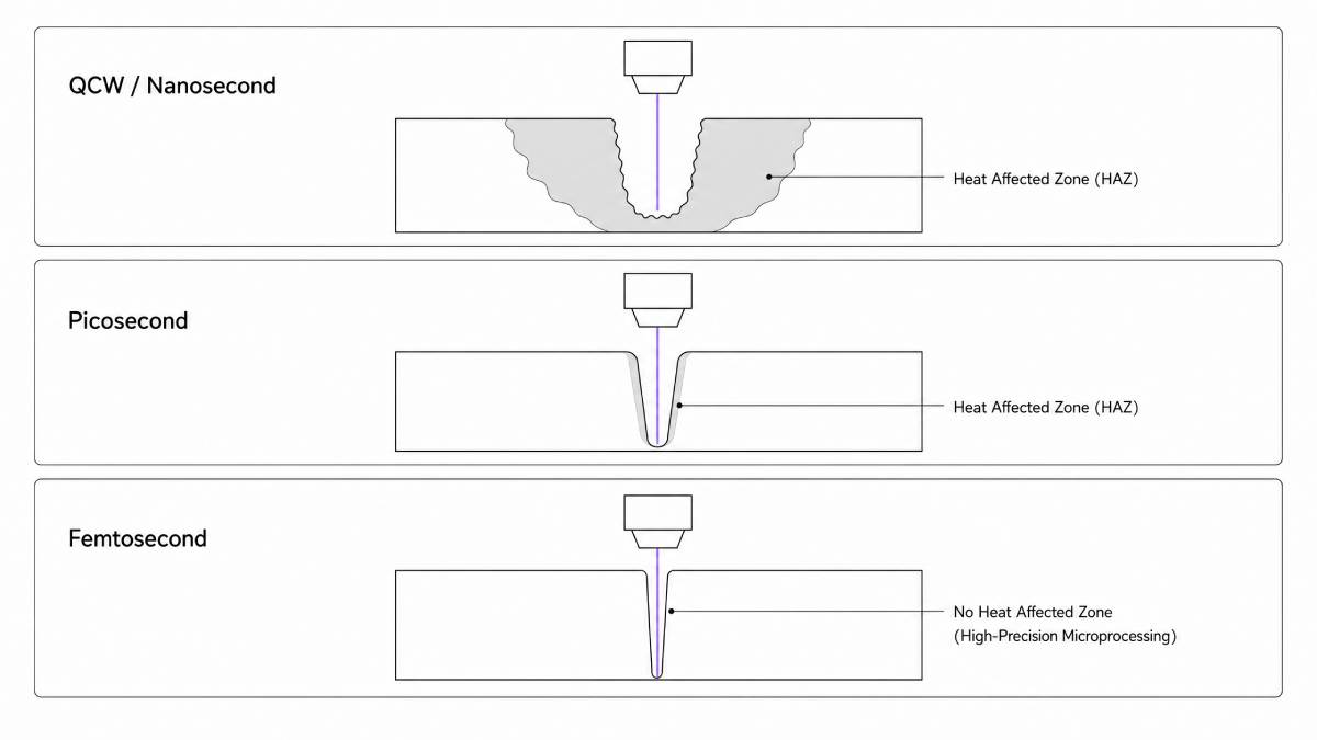
For manufacturers evaluating laser platforms, the choice is not purely between ultrafast categories. QCW (quasi-continuous wave) fiber lasers are frequently considered for the same wafer processing applications.
QCW fiber lasers deliver high peak power in millisecond-range bursts. They offer very high throughput and lower capital cost, and they are well-suited to applications where material removal rate is the primary metric and edge quality requirements are moderate — such as certain scribing and marking tasks.
However, QCW systems produce significantly more thermal side-effects than picosecond or femtosecond sources. For applications where HAZ must be minimized — thin wafer dicing, TSV drilling, fine scribing on sensitive device layers — QCW falls short of what ultrafast lasers can deliver.
The practical framework for selection:
QCW / nanosecond → cost-effective high-volume processes with relaxed thermal budgets
Picosecond → mainstream wafer dicing, scribing, and drilling where precision and productivity must be balanced
Femtosecond → premium microprocessing, hardest materials (SiC, sapphire), finest features, strictest HAZ requirements
For most production environments, picosecond laser systems represent the most deployable ultrafast solution today — offering substantially better process quality than nanosecond sources at a capital cost that has decreased significantly over the past decade.
Several converging trends in semiconductor manufacturing are driving continued adoption of ultrafast laser technology:
Wafer thinning continues as packages become more compact, pushing more processes into regimes where only laser-based techniques can maintain yield.
Advanced packaging architectures — fan-out, 2.5D interposers, chiplet stacking — require via densities and positional accuracy that laser processing is uniquely positioned to deliver.
SiC and GaN power device production is scaling rapidly for EV and industrial applications, creating sustained demand for laser slicing and dicing capabilities suited to these hard substrates.
Heterogeneous integration demands flexible processing across diverse material combinations in a single package, which laser systems handle better than single-material-optimized mechanical processes.
Across all of these trends, the common requirement is a laser platform that can be tightly controlled, rapidly reconfigured across material types, and operated with process stability in high-volume manufacturing environments.
Manufacturers increasingly require laser solutions that balance precision, productivity, and process stability for evolving semiconductor applications. Chanxan Laser provides precision laser processing solutions for wafer dicing, micro drilling, and brittle material machining across semiconductor and advanced manufacturing industries.
| Free solution
Previous: Why Is UV Laser Cutting the Industry Standard for Rigid-Flex PCB Depaneling?
Next: What Is a Nanosecond Laser System? Applications, Benefits, and Manufacturing Value