Key Words: Silicon Wafer Dicing PCB Depaneling Glass Cutting
Home > News > Industry News
【Description】:
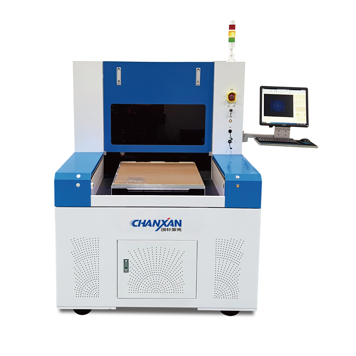
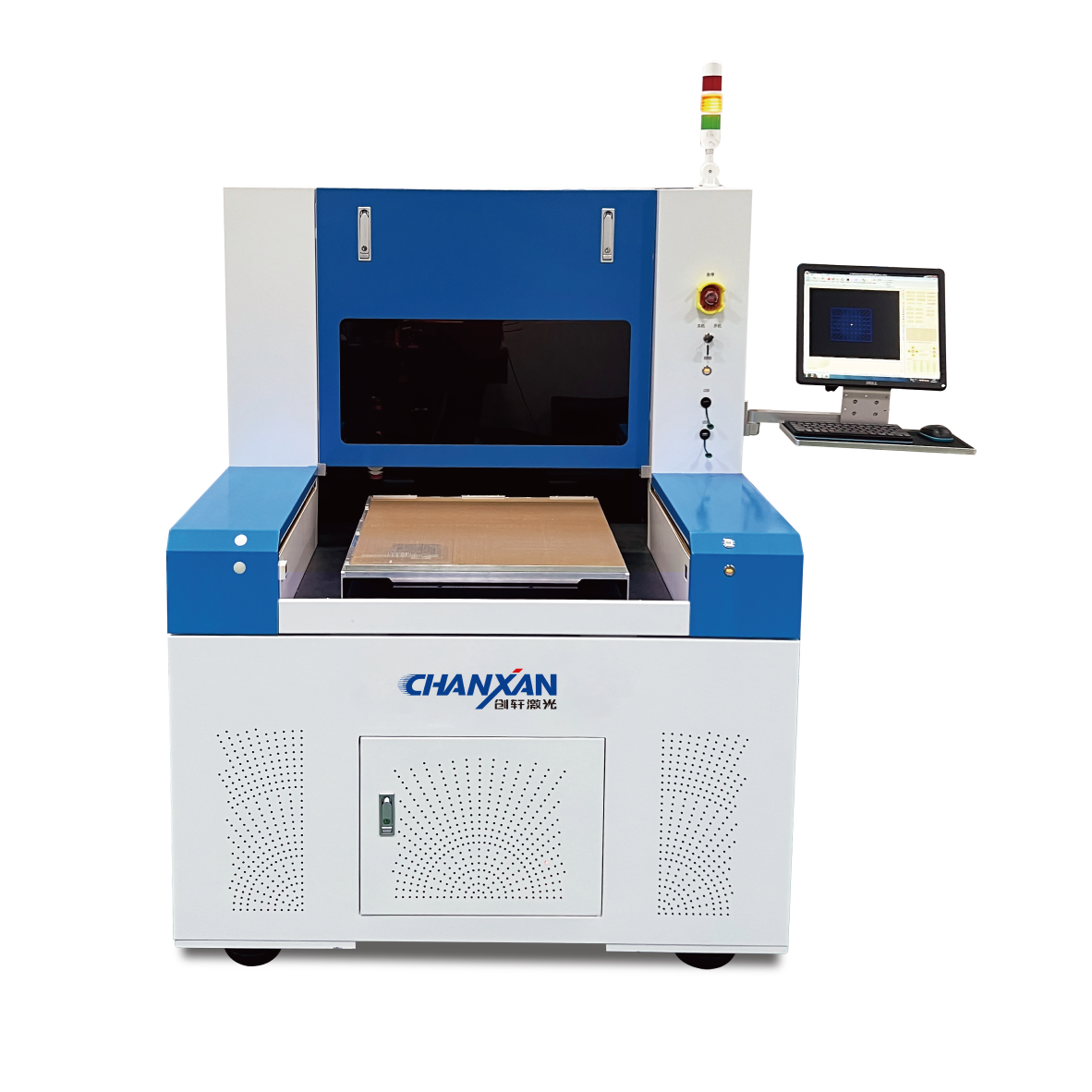
Chanxan picosecond laser dicing machine provides zero-kerf stealth dicing for brittle GaAs & InP wafers. Maximize die strength and optical surface quality for telecom lasers.
Gallium arsenide (GaAs) and indium phosphide (InP) form the definitive backbone of compound semiconductor technologies, driving a wide array of next-generation innovations. These materials are essential for high-frequency telecommunications—including 5G/6G, satellite communications, and radar—as well as optoelectronics like laser diodes, photodiodes, and VCSELs.
Furthermore, they power high-speed digital circuits for advanced computing and test equipment, enable optical communications via fiber optics, LiDAR, and sensing, and serve as the foundation for high-efficiency solar cells in space and concentrated photovoltaics. However, unlike traditional silicon, these compound semiconductors face a significant material hurdle: they are intrinsically brittle, presenting a unique fragility challenge during manufacturing and handling.
| Property | GaAs | InP | Silicon | GaN |
|---|---|---|---|---|
| Fracture Toughness (MPa·m¹/²) | 0.3–0.4 | 0.3 | 0.95 | ~1.5 |
| Hardness (GPa) | 7.0 | 5.2 | 11.0 | ~15 |
| CTE (×10⁻⁶/K) | 5.7 | 4.5 | 2.6 | 5.6 |
| Cleavage Planes | (110) | (110) | (111) | (10-10) |
| Bandgap (eV) | 1.42 | 1.34 | 1.12 | 3.4 |
| Thermal Conductivity (W/m·K) | 55 | 68 | 150 | 230 |
GaAs and InP have fracture toughness roughly one-third that of silicon. The same mechanical force that would cause a localized defect in silicon will cause catastrophic fracture in a compound semiconductor.
Cleavage planes: GaAs and InP both cleave along the (110) planes with exceptional ease. Mechanical blade dicing often propagates along these planes, leading to:
Delamination extending hundreds of microns from the cut
"Orange peel" edge morphology that reduces die strength
Chips that travel deep into the die area, causing catastrophic yield loss
Thermal stress sensitivity: The combination of low fracture toughness and moderate thermal conductivity means thermal stress from nanosecond laser dicing can exceed the fracture threshold. A 30°C temperature gradient can induce stress approaching the fracture toughness limit.
Surface quality requirements: For optoelectronic devices, the sidewall quality directly impacts optical performance. Rough or damaged sidewalls scatter light and reduce efficiency, especially for edge-emitting lasers and photodetectors.
Thin, large-area wafers: GaAs and InP are typically available in 100–150 mm diameters with 300–600 μm thickness. The brittleness combined with increasing wafer size makes handling and dicing a delicate operation.
| Parameter | Blade Dicing (GaAs/InP) | Nanosecond Laser | Picosecond Ablation | Picosecond Stealth |
|---|---|---|---|---|
| Kerf Width | 40–60 μm | 20–30 μm | 5–10 μm | N/A (0 μm loss) |
| Chipping | 10–30 μm | 5–15 μm | < 3 μm | < 1 μm |
| Cleavage Propagation | Extensive | Moderate | None | None |
| Heat-Affected Zone | N/A | 10–20 μm | < 3 μm | < 1 μm |
| Surface Roughness (Ra) | 0.5–1.5 μm | 0.2–0.5 μm | < 0.1 μm | < 0.05 μm |
| Stress Induced | High | Moderate | Very Low | Minimal |
| Post-dicing Cleaning | Required | Required | Minimal | None (stealth) |
| Optical Surface Quality | Poor | Moderate | Excellent | Excellent |
| Yield for VCSEL/Laser | 50–70% | 70–85% | 92–97% | 95–98% |
Industry Trend: For optoelectronics (VCSELs, photodiodes), where sidewall optical quality directly affects device performance, picosecond stealth dicing is rapidly becoming the standard. For power and high-frequency devices, both stealth and ablation are viable, with the choice depending on die size and street width requirements.
Why GaAs and InP are particularly suited for picosecond dicing:
High linear absorption at visible wavelengths: Both GaAs and InP have direct bandgaps in the near-infrared, meaning they absorb strongly at 1064 nm. This provides a significant advantage over silicon (which is mostly transparent) and wide-bandgap materials (which require nonlinear absorption):
Absorption depth at 1064 nm: GaAs ~1 μm, InP ~1.5 μm
This enables efficient energy deposition with moderate pulse energies
The surface absorption confines ablation to the near-surface region
Direct bandgap creates strong plasma formation: The high carrier mobility and direct bandgap mean that photo-excited carriers rapidly thermalize and recombine, efficiently transferring energy from the optical field to the lattice. This leads to efficient ablation with relatively low pulse energies.
Low thermal conductivity enables confinement: While the low thermal conductivity of GaAs/InP is a liability for nanosecond lasers (causing HAZ), for picosecond pulses it is actually beneficial. The 8 ps pulse deposits energy faster than it can diffuse, so the low thermal conductivity simply means the energy remains even more tightly confined — the limited "heat sink" effect prevents the HAZ from propagating.
Cleavage planes are inhibited by cold ablation: The picosecond pulse breaks crystal bonds via multiphoton ionization, thereby bypassing preferential cleavage planes. The material is vaporized/ionized before the stress wave can propagate along the cleavage direction.
For stealth dicing of GaAs/InP:
The high absorption at 1064 nm means focus must be positioned carefully to create a modified layer in the bulk without surface ablation.
Typical focus depth: 30–100 μm below the surface.
Multiple passes (2–3) at different depths create a continuous modified layer.
Tape expansion separates the dies with near-zero kerf loss and perfect vertical sidewalls.
This method is particularly valuable for expensive compound semiconductor wafers where every square millimeter counts.
Compound semiconductors (GaAs, InP, and their ternary alloys) represent the most challenging dicing application in semiconductor manufacturing. Their combination of extreme brittleness, cleavage plane propagation, and thermal sensitivity means that traditional dicing methods cause catastrophic yield loss. Even nanosecond lasers, which work for many materials, are insufficient for these fragile compounds.
Chanxan Laser's Picosecond Laser Wafer Dicing Machine is specifically engineered to meet the ultra-fine tolerances demanded by compound semiconductor devices. For AI and high-frequency computing applications, for telecom lasers, and for advanced sensing systems, our compound semiconductor dicing solutions deliver the yield and die strength required for commercial success.
Inquire our engineers for a free sample dicing test today| Free solution
Previous: Precision Laser Processing of Alumina (Al₂O₃) Ceramics: Substrate Dicing & Drilling Solutions
Next: Precision Laser Dicing for Glass Wafers and TGV Substrates