Key Words: Silicon Wafer Dicing PCB Depaneling Glass Cutting
Home > News > Industry News
【Description】:
How UV laser drilling enables 5G/6G LTCC substrates for RF front‑end modules and AiP. Via formation, cavity milling, and quality control for mmWave performance.
For engineers and procurement specialists who have selected LTCC green tape as the substrate platform for 5G/6G RF front‑end modules and Antenna‑in‑Package (AiP) designs, the critical challenge shifts from material selection to manufacturing precision.
At millimetre‑wave frequencies—24 GHz, 39 GHz, 77 GHz, and beyond—every via, every conductor edge, and every layer‑to‑layer transition directly impacts RF performance. Laser processing of LTCC green tape has become the enabling technology that transforms design intent into production‑ready substrates with high dimensional accuracy and repeatability.
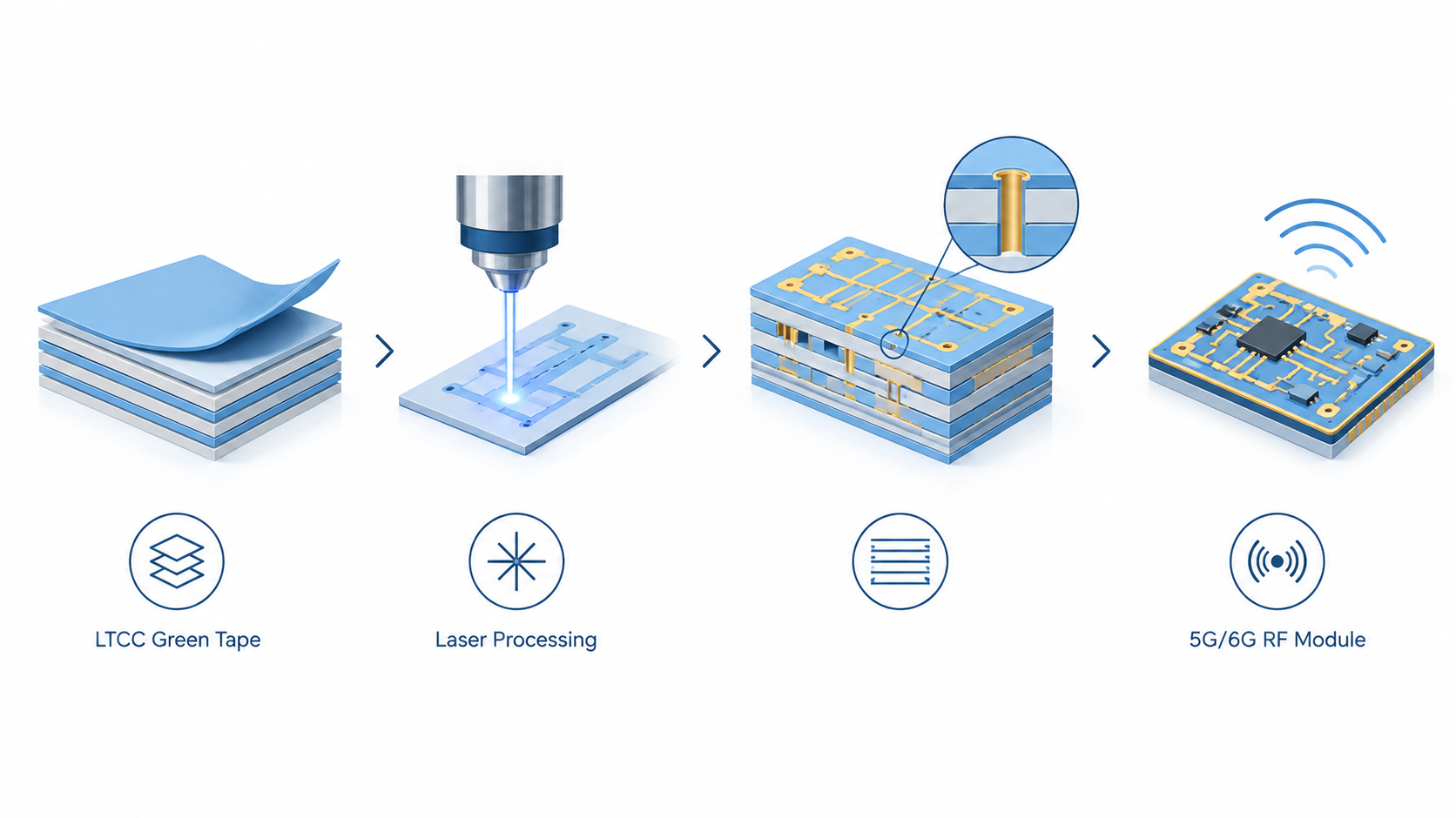
AiP integrates the antenna array directly into the package substrate, eliminating lossy cables and connectors. For 5G/6G AiP modules, LTCC provides low dielectric loss, multilayer capability, hermetic packaging, and effective thermal management.
±20 μm accuracy required to maintain phase coherence across the array.
Low‑loss RF signal paths connecting IC directly to the antenna.
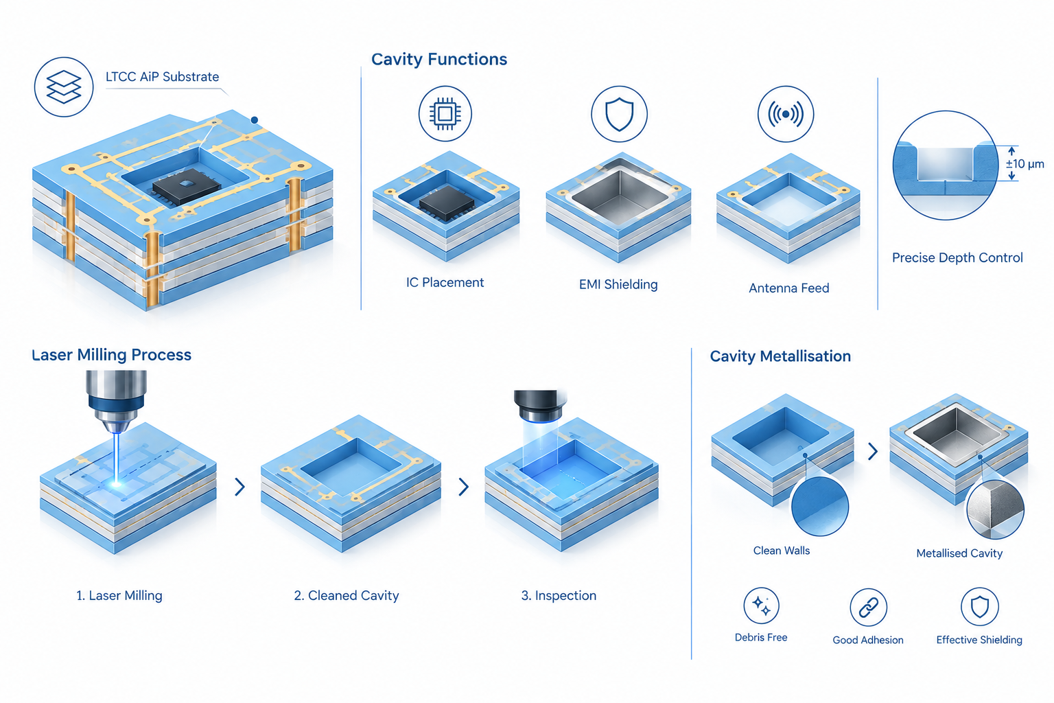
Precise recesses for IC placement and electromagnetic shielding.
In a typical 5G/6G RF front‑end module, vias serve multiple critical functions: RF signal transitions, ground connections, thermal dissipation, and impedance matching.
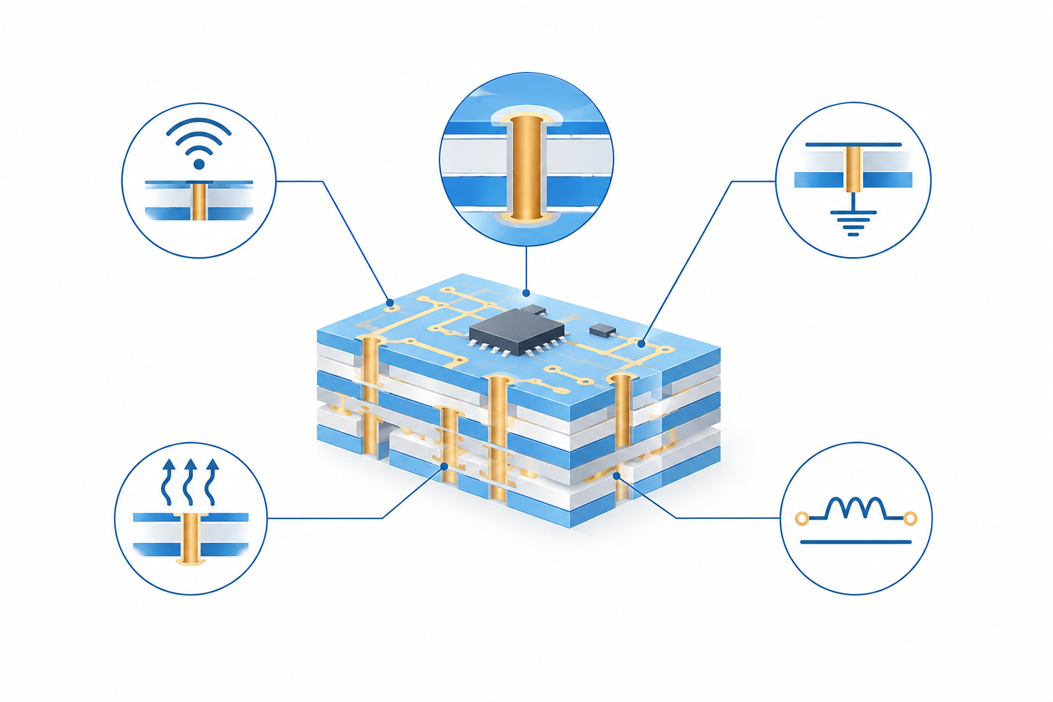
| Via Function | Typical Diameter | Aspect Ratio | Key Requirement |
|---|---|---|---|
| RF signal | 50–75 μm | 2:1 to 3:1 | Low loss, minimal parasitics |
| Ground | 100–150 μm | 2:1 to 4:1 | Low inductance, high density |
| Thermal | 100–200 μm | 3:1 to 5:1 | High conductivity, void‑free fill |
| Shielding | 75–100 μm | 2:1 to 3:1 | Continuous wall, no gaps |
Mechanical punching fails at 50–75 μm due to rapid tool wear and micro-cracks. UV laser drilling (355 nm) offers decisive processing advantages:
Fine via capability: Down to 30 μm diameter with excellent roundness.
Positional accuracy: ±20 μm with galvo scanners and vision alignment.
Post‑lamination drilling: Ensures perfect layer‑to‑layer registration after lamination.
Minimal HAZ: Nanosecond UV lasers limit HAZ to 10–20 μm; picosecond lasers reduce it to <5 μm.
Antenna‑in‑Package modules require recessed regions for IC die embedding, electromagnetic shielding, and specialized feed structures. Cavity depth tolerance must be strictly maintained within ±10 μm.
Laser cavity milling removes green tape material progressively using modulated UV beams. This delivers clean, debris-free cavity walls, promoting strong adhesion for silver paste metallisation and eliminating shielding voids.
LTCC is widely used for bandpass filters, low-pass filters, and duplexers in 5G/6G front‑end modules due to its low loss and ability to embed distributed elements.
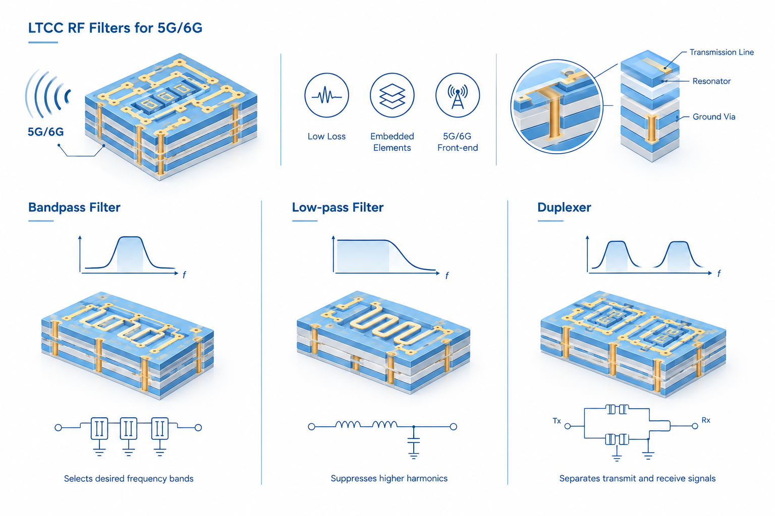
Via Placement Accuracy: Ground vias are positioned with high precision to define resonator boundaries.
Via Diameter Consistency: Uniformity prevents inductance variance and filter detuning.
Clean Via Walls: Debris-free walls reduce RF loss across high-frequency bands.
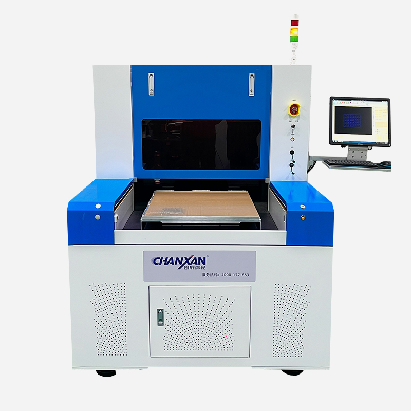
Chanxan Laser offers advanced UV nanosecond and picosecond laser systems purpose‑built for 5G/6G LTCC green tape processing. Whether you are developing 5G mmWave modules, 6G sub‑THz components, or AiP substrates for mobile devices, Chanxan Laser provides technology and industrial equipment to meet your production targets.
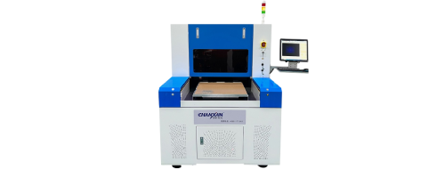
Contact Chanxan Laser application engineers today to discuss your processing requirements or request a sample drilling trial.
Contact Chanxan Laser Today| Free solution
Previous: Laser Drilling for Solid‑State Battery Separators: A Practical Guide
Next: Laser Processing for Automotive‑Grade LTCC Substrates: 77 GHz Radar and Power Electronics Packaging