Key Words: Silicon Wafer Dicing PCB Depaneling Glass Cutting
Home > News > Industry News
【Description】:
Discover how ultrafast lasers optimize Lithium Niobate (LiNbO3) and TFLN wafer processing. Eliminate edge chipping, delamination, and crack propagation in PIC optical modulator manufacturing.
In the rapidly evolving landscape of integrated photonics, accelerating the commercialization of next-generation transceivers requires substrate materials with extreme electro-optic efficiency. Among these, Lithium Niobate (LiNbO₃) has long been crowned the "silicon of optics." However, as the industry transitions toward Thin Film Lithium Niobate (TFLN) architectures and co-packaged optics, executing high-yield lithium niobate wafer dicing presents unprecedented challenges for traditional backend manufacturing lines.
To overcome the micro-fracturing, edge chipping, and delamination plaguing traditional diamond blades, high-precision lithium niobate laser cutting technologies have emerged as the industry benchmark. By leveraging ultra-short pulse picosecond and femtosecond laser engines, semiconductor manufacturers can achieve zero-stress singulation, enabling the high-density packing required for modern Photonic Integrated Circuits (PICs).
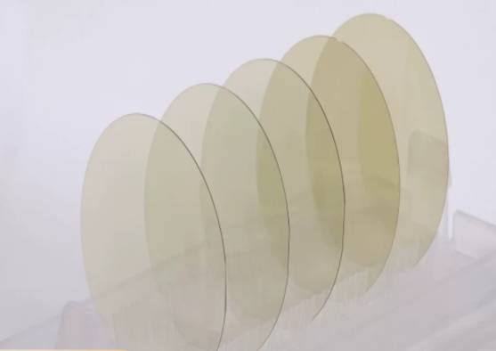
Lithium Niobate boasts unique physical properties that make it irreplaceable in ultra-high-bandwidth telecommunications and quantum computing networks. Its widespread adoption across the integrated photonics sector is driven by three foundational characteristics:
Superior Electro-Optic (EO) Modulation: LiNbO₃ exhibits a massive Pockels effect, allowing sub-volt control over light phases at frequencies exceeding 100 GHz—far surpassing the physical limitations of native silicon or Indium Phosphide (InP).
Exceptional Optical Transparency: It offers an incredibly wide transmission window spanning from 350 nm in the near-ultraviolet to over 5.0 µm in the mid-infrared, rendering it ideal for telecom C-band and O-band routing.
The TFLN Revolution: Thin Film Lithium Niobate bond-on-insulator wafers scale down optical mode sizes dramatically, allowing sub-micron sub-components to be tightly integrated alongside traditional Silicon Photonics platforms.
Despite its brilliant optical performance, Lithium Niobate is notoriously difficult to process. As a highly anisotropic, brittle crystalline material, conventional semiconductor dicing techniques inevitably introduce defects that severely limit manufacturing yield:
Extreme Brittle Cracking: Due to its strong crystalline cleavage planes, mechanical contact forces macroscopic fractures and subsurface damage (SSD), compromising the structural integrity of the entire PIC die.
Ultra-Thin Substrate Sensitivity: Modern TFLN functional layers are merely 300 nm to 600 nm thick, sitting on silica/silicon bases. The mechanical vibration of a blade easily triggers film delamination at the critical material interfaces.
Pyroelectric & Piezoelectric Sensitivity: LiNbO₃ generates massive localized electrical charges under rapid thermal fluctuations or physical stress, which can attract contaminants or trigger catastrophic electrostatic discharge (ESD) in surrounding microelectronics.
When evaluating mass production workflows for optical modulators and PIC assemblies, switching from mechanical blade dicing to advanced LiNbO₃ laser processing yields measurable performance gains:
Severe Edge Chipping: Blade friction forces jagged edge boundaries (> 10 µm chipping), scattering guided light and increasing insertion loss.
High Consumable Cost: Blade wear on hard crystals requires constant recalibration and frequent, expensive wheel replacements.
Fluid Contamination: Requires high-pressure deionized water cooling, risking chemical leaching or water spots on sensitive optical arrays.
Sub-Micron Quality: Non-contact "cold ablation" via multi-photon absorption limits the Heat-Affected Zone (HAZ) to under 2 µm, ensuring pristine side-walls.
Zero Mechanical Stress: Eliminates substrate cracking and prevents delicate thin-film delamination entirely.
Complete Design Freedom: Seamlessly processes curvilinear die profiles, expansion slots, and customized angled facets without tool restrictions.
Industrial-grade LN wafer laser dicing workstations deploy diverse optical configurations to execute complex manufacturing architectures within a single automated run:
Full-Thru Dicing & Singulation: Complete clean separation of thick bulk crystal blocks or heterogeneous TFLN stacks at high linear speeds without micro-cleaving.
Laser Grooving & Trenching: Scribing high-aspect-ratio optical isolation trenches to prevent parasitic crosstalk between high-density waveguide channels.
Edge Trimming & Facet Polishing: Direct laser polishing of die edges to optimize fiber-to-chip edge coupling, eliminating the need for hours of manual grinding.
Micro-Hole Drilling: Fabricating perfectly cylindrical vertical via holes and stress-relief ports with entrance diameters under 50 µm.
Precision laser singulation of Lithium Niobate serves as a core enabling process across major high-tech infrastructure and aerospace fields:
High-Speed Optical Modulators: Processing coherent 800G and 1.6T transceivers for long-haul telecom networks and hyperscale AI data centers.
Silicon Photonics Co-Integration: Precision-dicing hybrid TFLN-on-Silicon dies designed for multi-wavelength external cavity laser arrays.
Quantum Photonics: Singulating periodically poled lithium niobate (PPLN) waveguides dedicated to efficient entangled photon pair generation.
RF & Microwave Filters: Machining Surface Acoustic Wave (SAW) and Bulk Acoustic Wave (BAW) components for military and 5G/6G communication arrays.
Achieving defect-free, chip-free dicing on anisotropic crystals requires absolute control over pulse timing alongside an exceptionally rigid, vibration-isolated motion system.
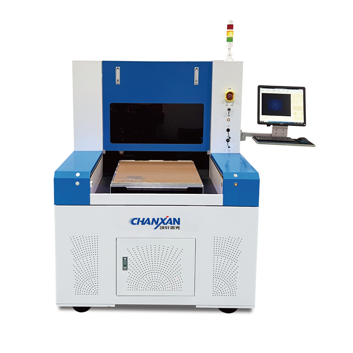
The Chanxan Ultrafast Wafer Processing System is custom-engineered to address the rigorous demands of industrial lithium niobate laser cutting. Built on a premium natural granite bed to eliminate low-frequency harmonic distortion, our system incorporates ultra-short pulse picosecond optics matched with closed-loop linear motor axis control.
Whether your enterprise is ramping up TFLN modulator volumes or deploying custom PPLN crystals for quantum computing grids, Chanxan provides the sub-micron volumetric tracking and cold ablation necessary to maximize fab yields.
Request an LN Wafer Processing Consultation & Application Quote| Free solution
Previous: Semiconductor Laser Dicing: Laser Ablation vs Stealth Dicing Guide
Next: BK7 Glass Laser Cutting and Micromachining for Precision Optical Manufacturing