Key Words: Silicon Wafer Dicing PCB Depaneling Glass Cutting
Home > News > Industry News
【Description】:
A technical guide for semiconductor backend engineers on choosing between laser ablation and stealth dicing based on wafer architecture, thickness, and sensitivity.
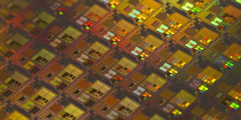
In the high-stakes world of backend semiconductor manufacturing, wafer singulation—the process of dicing a wafer into individual chips—is where the rubber meets the road. As wafers become thinner and chips shrink, traditional blade dicing is increasingly struggling with challenges like chipping, delamination, and excessive mechanical stress on delicate, ultra-thin substrates.
The industry has pivoted toward semiconductor laser dicing to solve these issues. Among the available technologies, two stand out: laser ablation and stealth dicing. Choosing the right path isn't just a technical preference; it’s a critical decision that impacts yield, throughput, and long-term device reliability.
Here is a guide to help you navigate the laser ablation vs stealth dicing decision.
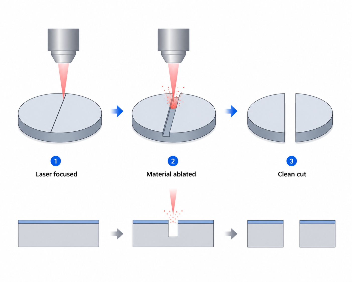
Laser ablation is a "top-down" direct machining process. A high-energy pulsed laser is focused on the wafer surface, where it vaporizes the material in the scribe line. By physically removing the material (ablation), the laser creates a clean cut through the wafer.
Grooving: Essential for Low-k (low dielectric constant) layers. Before traditional blade dicing, laser ablation removes the brittle surface layers to prevent cracking and delamination.
Full Cut: Excellent for standard thickness wafers where high-speed physical removal is required.
Complex Materials: Ideal for cutting through stacks of different materials (e.g., metal, passivation, and semiconductor) that require high energy to vaporize.
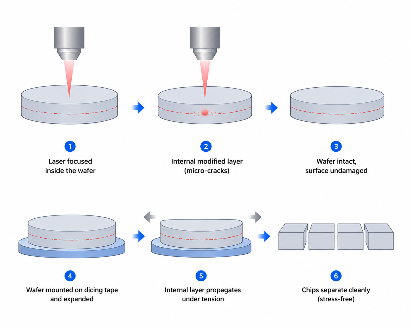
Unlike ablation, stealth dicing is a non-thermal, "dry" process that works beneath the surface. It uses an infrared laser that is transparent to the silicon wafer material. The laser is focused deep inside the wafer, where it creates an "internal modified layer" (micro-cracks).
The wafer remains intact at the surface until it is mounted on a dicing tape and expanded. The tension causes the internal modified layer to propagate, resulting in a perfect, stress-free separation of the chips.
Ultra-Thin Wafers: The go-to solution for wafers thinner than 100 μm.
Sensitive Structures: Perfect for MEMS, image sensors (CIS), and devices where debris or water-based cooling (required by blade dicing) could cause damage.
Zero-Kerf Requirements: Since no material is physically removed, the scribe line can be incredibly narrow, maximizing the number of dies per wafer.
To make an informed decision, you must evaluate how these technologies interact with your specific wafer architecture.
| Feature | Laser Ablation | Stealth Dicing |
|---|---|---|
| Process Type | Material removal (Vaporization) | Internal modification (Controlled cracking) |
| Material Loss (Kerf) | Moderate (10 ~ 30 μm) | Virtually Zero (< 5 μm) |
| Heat-Affected Zone | Significant (requires precision control) | Negligible (Cold process) |
| Debris | Produces vapor/particulates | Clean (Dry process) |
| Chip Strength | Good, but can have micro-cracks | Excellent (highest breaking strength) |
| Throughput | Faster for thick wafers | Faster for thin, sensitive wafers |
When deciding between laser ablation and stealth dicing, consider these three factors:
If your chips contain delicate micro-structures (like micro-lenses in CIS or moving parts in MEMS), steer clear of laser ablation. The debris and thermal impact are potential failure points. Stealth dicing provides a clean, dry, and impact-free environment that preserves the integrity of these delicate components.
If your wafer is a "sandwich" of different materials (e.g., thick metal layers on top of silicon), laser ablation is often superior. It can "clean" the path by vaporizing the top layers first, ensuring a smoother cut. Stealth dicing, which relies on the crystalline structure of the silicon, may struggle if the surface layers are too complex or opaque to the laser wavelength.
For thicker wafers (e.g., > 150 μm), laser ablation (or a hybrid groove-and-cut approach) is generally more efficient and cost-effective. However, as the industry pushes toward 30 μm or even thinner wafers, stealth dicing becomes the only viable option to achieve high yields without the risk of shattering the wafer.
In the modern semiconductor laser dicing landscape, there is no "one size fits all." Laser ablation is your heavy-duty, versatile workhorse for complex surface structures and thicker wafers. Stealth dicing is your precision instrument for high-value, ultra-thin, and debris-sensitive applications.
Often, the most advanced assembly lines don't choose just one; they employ a hybrid strategy—using ablation to pre-cut the surface and stealth dicing to separate the bulk—to squeeze every bit of efficiency and yield out of their silicon.
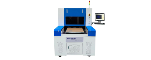
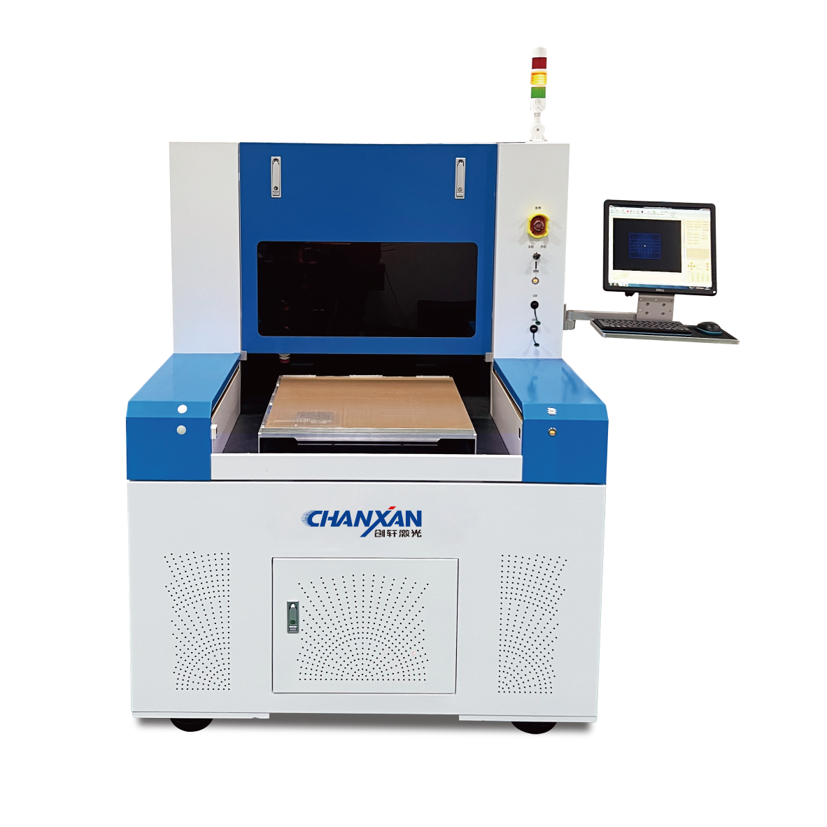
In laser ablation applications, managing the Heat-Affected Zone (HAZ) and eliminating debris redeposition are the ultimate challenges for packaging engineers. To address these pain points, Chanxan Laser has developed its state-of-the-art Picosecond Wafer Singulation Machine, specifically engineered for high-precision semiconductor backend processing.
By leveraging ultra-short pulse laser technology, Chanxan’s system redefines the capabilities of direct laser ablation:
Ultra-Narrow HAZ (≤ 3 μm): Utilizing picosecond-level pulses, the laser delivers energy so rapidly that the target material vaporizes instantly before thermal energy can conduct into the surrounding silicon crystal lattice. This "cold processing" capability restricts the Heat-Affected Zone to ≤ 3 μm, virtually eliminating the risk of micro-cracking and delamination.
Excellent Multi-Material Adaptability: Whether performing high-speed Low-k grooving, full-cutting of thin Si, GaAs, and GaN wafers, or scribing brittle sapphire and glass substrates, the Chanxan system ensures clean kerfs and flawless edge profiles.
Advanced Automation & Precision: Equipped with a high-resolution coaxial CCD vision alignment system and a high-speed linear motor gantry, the machine guarantees micron-level cutting accuracy and long-term stability for high-volume B2B semiconductor manufacturing.
| Free solution
Previous: Laser Dicing vs. Plasma Dicing: Which Wafer Cutting Technology Is Better?
Next: Lithium Niobate Wafer Laser Dicing for Photonic Integrated Circuits