
Key Words: Silicon Wafer Dicing PCB Depaneling Glass Cutting
Home > News > Industry News
【Description】:
Chanxan picosecond cold-ablation laser achieves burr-free singulation for semiconductor solder preform, minimizing heat-affected zone and raising production yield. It replaces traditional stamping for precision die-cut and semiconductor packaging manufacturers.
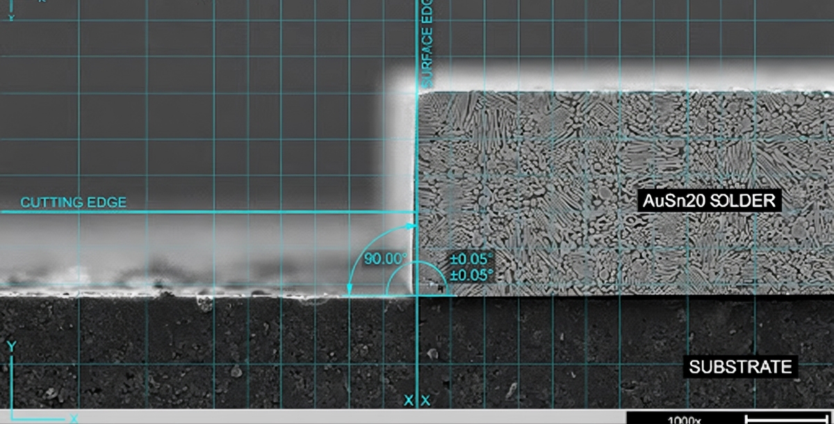
Solder preform is critical die‑attach bonding material widely used in semiconductor packaging, power electronics and high‑reliability hermetic sealing. Conventional mechanical stamping and nanosecond thermal laser easily generate burrs, heavy slag, phase segregation and large heat‑affected zones. These edge defects reduce assembly yield and raise post‑deburring cost for die‑cut service shops and semiconductor component manufacturers.
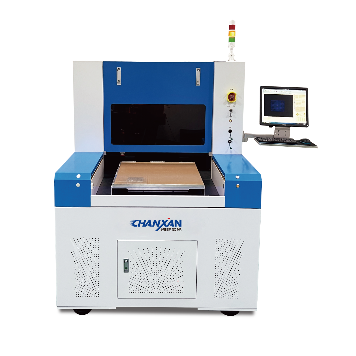
Chanxan provides optimized picosecond laser cutting machine for semiconductor solder preform, built for thin solder alloy, thin metal foil and flexible substrate processing. Sub‑10‑picosecond cold‑ablation mechanism vaporizes material without thermal melting conduction. It eliminates thermal segregation and edge burns, suitable for prototype sample development and continuous 24/7 fab mass‑production.
This ultrafast laser system solves typical manufacturing pain‑points of solder preform with industrial‑grade hardware configuration:
‑ True cold‑ablation processing, verified HAZ below 2 μm, prevents solder phase segregation and thermal deformation.
‑ Coaxial telecentric CCD vision positioning, supports complex custom outlines without expensive stamping moulds.
‑ Class‑00 granite vibration‑isolation platform plus ironless linear‑motor drive, stable micron‑level repeat accuracy.
‑ Zero post‑deburring required, helps factories achieve up to 99.8 % packaging yield.
Core technical parameters:
‑ Laser Source: Industrial Picosecond ultrafast laser
‑ Fiducial Positioning Accuracy: ±1 μm
‑ Cut‑edge Roughness: Ra < 0.1 μm
‑ Max processing speed: 3000 mm/s
For full technical specification sheet and configurable options, please visit our product detail page.
This picosecond laser system targets semiconductor packaging factories, precision die‑cut service providers and electronics manufacturing engineers. Processable materials cover AuSn solder preform, thin metal foil, PI film and FPC. Widely deployed for wafer‑level die attach, SMT substrate fabrication and ultra‑thin alloy foil stamping replacement.
Yes. Cold‑ablation delivers burr‑free clean edges. Secondary deburring steps can be removed from your production workflow.
No physical mould required. Only CAD drawings are needed for custom‑shape cutting, greatly shortening prototype sample‑development cycles.
Submit your solder‑alloy samples and CAD drawings for feasibility assessment, get technical proposal and formal quotation.
Contact Us| Free solution